Facebook
 Google
 GitHub
 Linkedin

Hi,
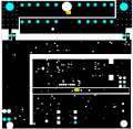
I am designing a 4 layer pcb board. For the GND layer I have given seperate GND ground for high current path(from transistors) which is connected to normal GND at a point.
I have given the seperate analog ground(AGND).
My professor commented like this:
If you only have analog parts over the analog GND then it is good that you are using a separate analog gnd but I am surprised that the analog part is so spread. A problem might be that your analog GND is connected at the end of the digital GND and digital noise will be added to your analog gnd. A start connection to the common GND separation might improve.
what does this mean?????
How can I add start connection???
I am adding image with this message
Regards
Vivek Alaparthi
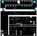
I am designing a 4 layer pcb board. For the GND layer I have given seperate GND ground for high current path(from transistors) which is connected to normal GND at a point.
I have given the seperate analog ground(AGND).
My professor commented like this:
If you only have analog parts over the analog GND then it is good that you are using a separate analog gnd but I am surprised that the analog part is so spread. A problem might be that your analog GND is connected at the end of the digital GND and digital noise will be added to your analog gnd. A start connection to the common GND separation might improve.
what does this mean?????
How can I add start connection???
I am adding image with this message
Regards
Vivek Alaparthi
Attachments
-
 35.1 KB Views: 21
Last edited: