 Facebook
 Google
 GitHub
 Linkedin
Hello everyone!
I'm designing a near field transmitter composed of a Pierce oscillator, a BPSK modulator, a power amplifier and a transmitting coil.
I'm having problems with the oscillator. The schematic is attached. The design was made by another student, who also fabricated a PCB for the oscillator and tested it.
The problem with the oscillator is that the output sine wave is asymmetric. This becomes a problem in the following stage (BPSK modulator), because when changing phases (from 0° to 180°) the sinewave is inverted (multiplied by -1). The result is a BPSK signal with an irregular envelope.
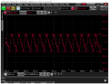
The schematic I have is the one used by the previous student who also fabricated and tested the PCB. I haven't tested the PCB myself, but in the results from the previous student the output signal from the PCB of the oscillator was centered in 0 V and was symmetrical.
I don't know how to solve this problem. I changed some parameters of the Pierce oscillator, but the problem persists.
I also attached the screenshot from the oscilloscope (from when the PCB was tested), and the datasheet of the quartz crystal used in the oscillator.
I'm designing a near field transmitter composed of a Pierce oscillator, a BPSK modulator, a power amplifier and a transmitting coil.
I'm having problems with the oscillator. The schematic is attached. The design was made by another student, who also fabricated a PCB for the oscillator and tested it.
The problem with the oscillator is that the output sine wave is asymmetric. This becomes a problem in the following stage (BPSK modulator), because when changing phases (from 0° to 180°) the sinewave is inverted (multiplied by -1). The result is a BPSK signal with an irregular envelope.
The schematic I have is the one used by the previous student who also fabricated and tested the PCB. I haven't tested the PCB myself, but in the results from the previous student the output signal from the PCB of the oscillator was centered in 0 V and was symmetrical.
I don't know how to solve this problem. I changed some parameters of the Pierce oscillator, but the problem persists.
I also attached the screenshot from the oscilloscope (from when the PCB was tested), and the datasheet of the quartz crystal used in the oscillator.
Attachments
-
 185 KB Views: 27
 -
1.7 KB Views: 16
-
276.6 KB Views: 12


