Need help understanding this current sensing design

Thread Starter

alobaolalekann

Joined Jan 31, 2017
21
I'm using this inverter reference design from TI for my design but I'm unsure of how to correctly sense the circuit current.

As shown in the provided schematic below, they use hall effect sensor.
For my own design, I'm using current transformer but I'm unsure if the interfacing to the microcontroller would be pure dc or ac(with positive offset). Which is okay for the control?
If it would be the ac, is it at the line frequency or the switching frequency of the full bridge?

Thank you.
1707142848806.png
 

Reloadron

Joined Jan 15, 2015
7,580
This would go much better with a more legible schematic.

Using a Current Transformer make sure it is never left open circuit with current flow in the primary. You always want a burden resistance when using a Current Transformer. How much current do you plan to measure? Have you considered other things like a current transducer and how much AC current did you plan to measure?

Ron
 

Thread Starter

alobaolalekann

Joined Jan 31, 2017
21
Here is another schematic. Hopefully it makes better sense.

1707148719978.png

Questions I have:
1. Is the current transformer going to work at the output frequency or the switching frequency?
2. Is the output of the CT that interface with the MCU going to be pure DC or an alternate signal?

Thank you.
 

Reloadron

Joined Jan 15, 2015
7,580
What exactly are you trying to do? That schematic makes no sense at all.

A CT Current Transformer like any transformer is designed to work at a specific frequency, for example 50 Hz and 60Hz are popular. I told you a CT needs a burden resistance. I suggest you read up on current transformers, their use and signal conditioning for them.

Ron
 

Thread Starter

alobaolalekann

Joined Jan 31, 2017
21
I am not exactly bothered about how CT works, I think I know.

What I need clarification on is
1. whether it will be placed before or after the capacitor(inline with the 240VAC,50Hz output). My understanding is that the frequency before and after the LC filter is different and getting to know where is best suitable will help to select the correct CT in the appropriate frequency range.

2. For anyone with experience designing digital high frequency inverter, which type of signal conditioning from the CT ouput is better for the inverter system control. I have the option of adding a positive offset to remove the negative aspect of the induced ac in the CT output before inputting to the microcontroller or I could rectify the CT output signal to pure DC before inputting it to the MCU
 

Alec_t

Joined Sep 17, 2013
14,430
1) If the CT is designed for 50/60Hz working then you connect it at the 240V output, after any filtering to reduce/eliminate switching frequencies.
2) I can't see any obvious reason why one way would be better than the other.
 

Thread Starter

alobaolalekann

Joined Jan 31, 2017
21
1) If the CT is designed for 50/60Hz working then you connect it at the 240V output, after any filtering to reduce/eliminate switching frequencies.
2) I can't see any obvious reason why one way would be better than the other.
On (2); adding diodes for rectification might introduce some inefficiency in the computation as you might have to start to consider the forward voltage drop in your calculations
 

Reloadron

Joined Jan 15, 2015
7,580
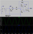
If you want to amplify and measure a CT output you want a circuit like this:

Current Transformer Amp2.png

Now in the above the burden resistance would be R1. CT outputs are normally a ratio of primary current to secondary output current. Depending on your uC A/D if you plan on using a uC for example an Arduino using an Atmega 328P or similar you cannot feed any signal going below 0 VAC into an A/D channel so we need to place the AC signal on a DC component above the 0.0 volt baseline. This offset is accomplished by R3 and R4 in the above schematic. Not all uC require this as some handle a negative signal just fine. The Vout signal is shifted to a 2.5 VDC baseline. The offset in this case is based on an Arduino UNO Rev 3 where the A/D has a 5.0 volt reference. Using code we find the peaks and calculate the peaksand derive the RMS voltage value which is proportional to the actual current in the primary of the CT. I see no need to rectify anything.

Ron
 

Thread Starter

alobaolalekann

Joined Jan 31, 2017
21
If you want to amplify and measure a CT output you want a circuit like this:

View attachment 314597

Now in the above the burden resistance would be R1. CT outputs are normally a ratio of primary current to secondary output current. Depending on your uC A/D if you plan on using a uC for example an Arduino using an Atmega 328P or similar you cannot feed any signal going below 0 VAC into an A/D channel so we need to place the AC signal on a DC component above the 0.0 volt baseline. This offset is accomplished by R3 and R4 in the above schematic. Not all uC require this as some handle a negative signal just fine. The Vout signal is shifted to a 2.5 VDC baseline. The offset in this case is based on an Arduino UNO Rev 3 where the A/D has a 5.0 volt reference. Using code we find the peaks and calculate the peaksand derive the RMS voltage value which is proportional to the actual current in the primary of the CT. I see no need to rectify anything.

Ron
Thank you!
 

MisterBill2

Joined Jan 23, 2018
19,588
The current ripple thru the CY will be at the switching frequency As it will drop towards zero each time the transistors switch. Because of all the shunt capacitors at the input, I assume that the supply is DC. So there will be a bit of DC in the CT
 
Top