My first PCB – ESP32-C3 RC controller (7th-grade student)

Thread Starter

Ryan Jun

Joined Jul 24, 2026
1
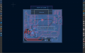
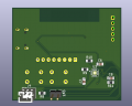
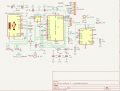
Hi! I’m a 7th-grade student, and this is my first PCB design. It is a rechargeable BLE RC car controller made with KiCad.
It uses an ESP32-C3, USB-C, a BQ24074 LiPo charger, and an AP2112K 3.3V regulator. ERC and DRC show no active errors, but I have not ordered the PCB yet.
Could you please check my schematic and PCB layout for any mistakes, especially the power circuit, USB-C connections, grounding, and ESP32 antenna area?
I’m still a beginner, so simple explanations would be greatly appreciated. Thank you!
스크린샷 2026-07-24 115540.png스크린샷 2026-07-24 115337.png스크린샷 2026-07-24 115427.png스크린샷 2026-07-24 115540.png스크린샷 2026-07-24 115549.png
 
Last edited by a moderator:

panic mode

Joined Oct 10, 2011
5,129
spread the symbols in schematics a bit more,
do not draw diagonal wires,
do not have things overlap - it makes schematics unreadable,
keep connections short (why is R11 so far away when it could be next to R10?),
why not turn R1, R2 vertically (like R10), same goes for most of the passives. in fact of all R and C i would only keep R6 and R7 horizontal.
why cram PWR_FLAGs into busy part of schematics when upper right corner is wide open?
GND and negative voltage symbold should point down, positive should point up - always (see the +3V3 next to R4. GND next to C2 and SW2 etc.)
why use wirelabels on C1,C2 instead of just conencting them by wire? make the schematics connected so we can follow the wire to see where it goes. all those single parts at the bottom are great example of what not to do. it took me FOREVER to see that U2 pin3 connects to R8.

differential pairs need to be named accordingly to KiCad convention, for example left side of R6 and R7 can be called USBD+, USBD-.
wires on the right side can be called D+,D-. they need to be routed as differential pair.

once you have schematics in readable form, i will take another look.

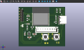
about PCB... i am just used to complaining when i see no mounting holes. because sooner or later you will want to attach the board to something (enclosure, whatever) and then you will be scratching your head what to do.
guess how much cleaner that wide track near C3 would be if you rotated C3 180deg. also i like to move buttons away from anything that is tall or otherwise in the way, such as that white JST connector.
also SW1, SW2 just enumerated buttons. it would be better to move those away or hide them and add new labels that specify what the buttons are for (BOOT, RESET). because other than you nobody else has any clue what they are from the look at PCB.
 
Top