Facebook
 Google
 GitHub
 Linkedin
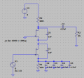
Hi there, I am working with a HEMT schematic (design attached) on LTSpice (I only have beginner experience with it) and I would like to find out a few things about this circuit:
1. The amplification factor and dissipated power and how they depend on the operating point for the transistors
2. The bandwidth of the circuit for a range of input resistances, inductances, capacitances, etc.
3. Is there a way of modelling noise for the transistors?
I currently have a bode plot going for the schematic, and can see currents and voltages at different points of the circuit as a function of frequency. Is there also a way to include power dissipated in these plots? I can find the find the average power for various components, but how can I find the total power dissipated by the circuit? For amplification factor, what would I use as the output voltage? How do these depend on transistor conditions?
Thanks.
Attachments
-
 8 KB Views: 20