Lexicon Pcm41 repair

Thread Starter

bt63

Joined Jul 16, 2024
21
Hi,

I'm trying to repair a PCM41 that has no delay signal at all when the mix control is turned fully wet.

I've been probing the circuit and comparing measurements with the help of Claude, but at this point it feels like I'm going in circles. Fortunately, I have a second, fully working PCM41 that I've been using as a reference to compare signals and voltages throughout the circuit.

To rule out faulty ICs, I've swapped every socketed chip from the non-working unit into the working unit. The working unit continued to function normally with every chip installed, which strongly suggests the ICs themselves are not the source of the problem. I've also completely recapped the non-working unit.

I feel like I made some headway with the unit, and determined that it seems that the sample and hold function u23, theres no input or output from it, so im thinking its this part thats not working correctly somethings I found. Mostly in the C4/D4 section of schematic 4

  1. R102 connected to q4 is severely under voltage compared to the good unit
  2. 95, show 15 volts on both sides, instead of just one side. The good one shows 3volts
  3. I get signal on pin 6 of u22 but none of the others on that IC, I know these work in tandem so I'm not sure if thats nice clue or not?

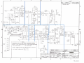
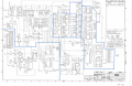
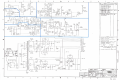
Also here's the schematic. I have a scope, and multimeter, but don't have the signature analyzer as well!


Thanks Any help would be appreciated !!!

https://audiocircuit.dk/downloads/lexicon/Lexicon-PCM41-ddp-sm.pdf
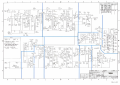
2Schematic.png4Schematic.png1Schematic.png3Schematic.png\
 

spenkmo

Joined Apr 24, 2025
38
The section you focused on is the sample-and-hold stage of the ADC. The sequence of operation looks like the following:
  1. U46/P15 outputs a high duty-cycle waveform called ISAM/ in the schematic, roughly 0-3.5V peak-to-peak (TTL level).
  2. The wave drives Q4 through R102. Q4/C should have a inverted and low duty-cycle waveform, roughly 0-15V peak-to-peak.
  3. The Q4 output controls the switches in U23. There are two states:
    1. Q4 output high (sample): Switches U23/P1-P2, U23/P8-P9 and U23/P11-P10 are on, the input analog signal (left of R94) is reversely followed by OPAMP U22.
    2. Q4 output low (hold): Switch U23/P4-P3 is on; the input analog signal is shut off from the OPAMP. The OPAMP holds its output value due to C101.

If the voltage across R102 is severely lower than the good unit, Q4 should be mostly off and its output is high. However, that contradicts what you observed on the voltages on the two sides of R95. Are you sure you measured R95 not R96? It's possible that R95 is shortened though. In terms of U22 output having signal, that's actually expected. As U22 is an OPAMP working in negative feedback mode, its input U22/P2 and P3 are supposed to be nearly constant.

It's worth comparing the waveform of U46/P15 (or the left side of R102) between the two units. If the same, we really narrow down to R102 and Q4. Otherwise, we have to look further back.
 

Thread Starter

bt63

Joined Jul 16, 2024
21
could have been R96. I measured both units, and the readings between the good and bad unit didn’t match, which made me suspect it. I was also able to see signal passing through one of the resistors — I don’t remember exactly which one, but I believe it was the lower resistor, R96.

It seems like U46 pin 15 is low compared to the good unit. I can see a pulsing signal there, similar to the good unit, but it’s very blurry and much lower in amplitude. I have to set my scope down around 0.5 mV to see it clearly.

I’ve been trying to trace the signal back through the circuit to find where it originates and where the chain is breaking, but I’m having trouble following the schematic and understanding how the signal feeds through the different chips.
 

spenkmo

Joined Apr 24, 2025
38
Based on your measurement, it looks like U46/P15 is just 0V with some noise. U46 (LS374) has three-state outputs, controlled by U46/P1 (~OE). U46/P1 is tied to GND so U46/P15 shouldn't be high-impedance. But it's worth verifying U46/P1 is secured to GND indeed. Also, it may be helpful to browse through other outputs of U46 (like P2, 5, 6, 9, 12, 16, 19) to see if they have similar symptom. If so, U46 may be bad.

If ~OE is good, we may further check U46/P11 (CLK) to see if it has the same clock pattern as the good unit.

If the clock is good, then compare the waveform of U46/P14, which is the data input to the flop that outputs through a three-state buffer to U46/P15. A mismatch here indicates the problem is further back.
 

Thread Starter

bt63

Joined Jul 16, 2024
21
All the pins show a low-level signal like pin 15, except for pin 11, which has a clock signal.
If the clock is good, then compare the waveform of U46/P14, which is the data input to the flop that outputs through a three-state buffer to U46/P15. A mismatch here indicates the problem is further back.
These should have the same signal?

I also swapped all of the ICs into the good unit, and they all work there, so I don't think the IC itself is faulty.

One thing I'm still trying to understand is the signal flow. U23 seems like the start of the digital section, but from your earlier advice it sounds like it isn't. I've traced the signal downstream through U35 and U41, but I'm not sure where it goes after that. Both ICs receive the same weak signal, and the other pins show weak activity as well.
 
Last edited:
If all the output pins of U46 are low but the clock on U46/P11 is fine, then all the input pins of U46 (eg, P3,4,7,8,13,14,17,18) must be low too. If this can be confirmed, we must trace further back to 32x8 ROM U47 (82S123). Otherwise, U46 is where the problem occurs. It doesn't mean the U46 chip is bad, as your swapping test proved it's okay. It could be the socket or PCB wires. Especially at U46/P1, the ~OE (tri-state output control) and U46/P20 and P10 (the VCC and GND pins). Any loose connection of these pins could ruin the operation of the chip.

U23 is a quad-analog-2:1-switch device, merely selecting different analog paths to feed OPAMP U22. The digital controlling signal, the output of Q4, can be traced back (ISAM on the schematic) to ROM U47 that stores the waveform pattern, registered by U46. The ROM's address is sequenced by half of U44, a dual-binary-counter.
 

Thread Starter

bt63

Joined Jul 16, 2024
21
So I tested U46. Pins 1 and 10 are grounded, and pin 20 has +5 V, so the power rails look correct. That makes me wonder if U47 is the next likely suspect.

I've checked U47 before, and the results have been consistent: the clock appears to be functioning, but both the inputs and outputs seem dead.

Claude suggested jumping a few connections, and I was able to get some noise out of the unit. However, it was only digital garble along with a VCO-style sweep/whine—no recognizable delayed audio. This freaked me out, because I wasn't sure if the jumps were actually safe, and desoldered


U23 is a quad-analog-2:1-switch device, merely selecting different analog paths to feed OPAMP U22. The digital controlling signal, the output of Q4, can be traced back (ISAM on the schematic) to ROM U47 that stores the waveform pattern, registered by U46. The ROM's address is sequenced by half of U44, a dual-binary-counter.
Ah! I'm starting to get it Thanks!
 

spenkmo

Joined Apr 24, 2025
38
I've checked U47 before, and the results have been consistent: the clock appears to be functioning, but both the inputs and outputs seem dead.
Did you mean you had checked U46 before. U47 doesn't have a clock. It's a ROM.

Yes, it appears that U46 doesn't get any meaningful inputs from U47. So we should check all U47's inputs. U47/P10,11,12,13, the four lower address inputs are driven by counter U44. These should toggle; otherwise U47's output would stay constant. Another thing to watch for is U47/P15 (~CE). It's the tri-state output control. U47/P15 is tied to GND but worth double-checking.

If U47/P10-13 are not toggling, then U44 should be checked next.
 
Top