I want some suggestions or help in SPI interfacing.

Thread Starter

Gouthama Priyan

Joined Jul 27, 2018
50
You make life difficult. Why do you want SPI interface between PC and the 'outside' world?
SPI sort distance and very sensitive for external electrical noise.

Look at the microchip site there are some SPI timing descriptions available.

Most simple way is to use a PIC from PC => PIC parallel in SPI master / slave or serial ( data in or out or both.)
Picbuster
Hello I just got through your comments
i want some suggestions or help in SPI interfacing.
Actually i wanted to do some paramter setting in LV8907 IC, where the parameter settings are done through SPI interface. Could you suggest me an method to carry out parameter setting?


Mods Note:
Please don't hijack other member's thread.
This thread was split from Talking to SPI devices from parallel port.
 
Last edited by a moderator:

Thread Starter

Gouthama Priyan

Joined Jul 27, 2018
50
I would like to communicate with LV8907
And i'm new to this
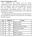
i have added a screenshot of device configuration of the IC for your reference
Could you please suggest how we could store the settings in OTP
upload_2019-9-23_21-41-40.png
 

jpanhalt

Joined Jan 18, 2008
11,087
Those are the standard 4 lines ( not all are necessarily used) for SPI. The question was, what MCU (microcontroller) are you using and what language? The only MCU I am familiar with are 8-bit PIC from Microchip; although, for SPI there is a lot of similarity in function. I just can't give much help in identifying the registers.

Just looking at the table you post:
1) EN means the chip needs to be enabled. It has nothing to do with SPI per se, except you cannot communicate with a chip that is not enabled.
2) CSB is chip select. It usually requires a single bit to be set or cleared. Like enable, it is active when low and idles high. That active when low is often indicated by a line over the identifier (\(\small\overline{CSB}\) )or a leading "!." !SS (slave select) and !CS (chip select) are other names for that function. It could be written !CSB too. When it is low, the chip knows the Master (MCU) is communicating with it.
3) SCLK is the clock from the MCU. It keeps everything -synchronous.
4) SI are communications form the master to the slave. The digital message will tell the slave whether the master is writing to a slave register or reading a slave register. It goes by other abbreviations, including MOSI (master out slave in) and SDI (serial device in from the slave perspective).
5) SO is the line on which the slave sends to the master. Other abbreviations are MISO (master in slave out) and SDO (serial device out). SDI/SDO abbreviations can be a bit confusing as they change with ones perspective (i.e., slave or master).
 

Thread Starter

Gouthama Priyan

Joined Jul 27, 2018
50
upload_2019-9-24_10-5-0.png

This is information regarding device configuration with SPI and OTP writing for LV8907.
Yes you can help me with 8 bit PIC m/c with your preferred language.
I'm pretty much new in this SPI & OTP writing.
could you suggest me how to startup and proceed with
I have a set of minimum registry settings to be added to the IC through OTP writting.
If you could help me with SPI configuration OTP writing procedure, It will be very helpful in configuring the IC
Thanks in advance
Those are the standard 4 lines ( not all are necessarily used) for SPI. The question was, what MCU (microcontroller) are you using and what language? The only MCU I am familiar with are 8-bit PIC from Microchip; although, for SPI there is a lot of similarity in function. I just can't give much help in identifying the registers.

Just looking at the table you post:
1) EN means the chip needs to be enabled. It has nothing to do with SPI per se, except you cannot communicate with a chip that is not enabled.
2) CSB is chip select. It usually requires a single bit to be set or cleared. Like enable, it is active when low and idles high. That active when low is often indicated by a line over the identifier (\(\small\overline{CSB}\) )or a leading "!." !SS (slave select) and !CS (chip select) are other names for that function. It could be written !CSB too. When it is low, the chip knows the Master (MCU) is communicating with it.
3) SCLK is the clock from the MCU. It keeps everything -synchronous.
4) SI are communications form the master to the slave. The digital message will tell the slave whether the master is writing to a slave register or reading a slave register. It goes by other abbreviations, including MOSI (master out slave in) and SDI (serial device in from the slave perspective).
5) SO is the line on which the slave sends to the master. Other abbreviations are MISO (master in slave out) and SDO (serial device out). SDI/SDO abbreviations can be a bit confusing as they change with ones perspective (i.e., slave or master).
 

Thread Starter

Gouthama Priyan

Joined Jul 27, 2018
50
Those are the standard 4 lines ( not all are necessarily used) for SPI. The question was, what MCU (microcontroller) are you using and what language? The only MCU I am familiar with are 8-bit PIC from Microchip; although, for SPI there is a lot of similarity in function. I just can't give much help in identifying the registers.

Just looking at the table you post:
1) EN means the chip needs to be enabled. It has nothing to do with SPI per se, except you cannot communicate with a chip that is not enabled.
2) CSB is chip select. It usually requires a single bit to be set or cleared. Like enable, it is active when low and idles high. That active when low is often indicated by a line over the identifier (\(\small\overline{CSB}\) )or a leading "!." !SS (slave select) and !CS (chip select) are other names for that function. It could be written !CSB too. When it is low, the chip knows the Master (MCU) is communicating with it.
3) SCLK is the clock from the MCU. It keeps everything -synchronous.
4) SI are communications form the master to the slave. The digital message will tell the slave whether the master is writing to a slave register or reading a slave register. It goes by other abbreviations, including MOSI (master out slave in) and SDI (serial device in from the slave perspective).
5) SO is the line on which the slave sends to the master. Other abbreviations are MISO (master in slave out) and SDO (serial device out). SDI/SDO abbreviations can be a bit confusing as they change with ones perspective (i.e., slave or master).


If required i have attached the datasheet of the IC LV8907, for your reference. If possible could you read and let me know what is the type of spi required and what process of OTP writing shall be preferred for registry and parameter setting for minimum functionality of the IC
 

Attachments

jpanhalt

Joined Jan 18, 2008
11,087
There is a lot there to go through. I just took a brief look. There is nothing particularly unusual about the SPI. It appears to be Mode 0 (leading edge clock rising, data changes on falling edge, page 20 of the DS), which is very common. The chip is designed to work standalone. That is, without an MCU. However, changing any of the defaults and monitoring some of the operating registers will require an MCU.

The chip has 2 modes: standby and normal. Programming and full SPI communication can only be done in standby mode (EN = low) and VS >= 14 V. When EN is high, the chip is in normal mode (i.e., controlling a motor), but some of the OTP status registers can still be read in that mode. I am unsure whether VS needs to be >=14 V for those reads or whether then can be read at 12 V too. I suspect the latter.

Despite the high voltage to the chip, on-board regulators provide power for external devices at either 3.3 V or 5 V and up to 50 mA . That should be adequate for most MCU's. The SPI data and clock lines typically run at 3.3 V. (I didn't see any statement that those voltages change when the voltage regulator for the external device is changed to give 5V output. That would be nice to know if you plan to use a 5 V MCU.)

Start-up settings are stored in non-volatile "OTP" registers. Normally OTP means "one time programmable." However, there is a register bit to "lock" the OTP contents. That action is irreversible. The datasheet says that OTP registers "should" only be reprogrammed once. That does not mean they can only be programmed once. In fact, the manual for the evaluation board (https://www.onsemi.com/pub/Collateral/LV8907UWGEVK_USER_GUIDE.PDF.PDF ) suggests they can be reprogrammed at least a few times so long as the locking bit is not set. That evaluation board is "arduino compatible."

At this point, I am not sure of what questions you have. Have you ever set up SPI with a microcontroller? Do you know about setting SPI mode? Do you have the evaluation board? Do you really need to change the default settings?

I have code for a PIC written in Assembly, Presumably almost any MCU can be used with the LV8907. As mentioned above, it would be nice to know whether those pins are 5 V tolerant.
 

Thread Starter

Gouthama Priyan

Joined Jul 27, 2018
50
Yes it is designed to work standby.
But provided few registry settings has to be stored on OTP memory through SPI interface was mentioned.
Other than that more complex is not required as of now
The minimum registry settings needed to be stored in OTP memory are as follows,
upload_2019-9-24_16-26-50.png
It is recommended to keep Vs> 14V
And which pins you are requesting about 5V tollerant.
Could you be more specific?
With your PIC written code could i be able to do registry setting of the above mentioned with that IC.
Let know. Yes i'm pretty new haven't tried setting up SPI with m/c before.
 

jpanhalt

Joined Jan 18, 2008
11,087
As previously stated (post #7),
The SPI data and clock lines typically run at 3.3 V.
Actually, on reviewing the evaluation board (snippet below), it seems all of the relevant pins must be 5 V tolerant:
upload_2019-9-24_7-31-5.png

The ones used for SPI (using the labels here) are, SO, SI, SCLK, CSB, and EN. Note, those with pullup resistors are pulled to 5V.

Since you asked, here are my basic utilities for reading and writing using SPI (MCU= PIC16F17830, device = thermocouple amplifier)

Code:
;*******************************************************************************
;SPI read/write utilities
;*******************************************************************************
PutAddr                       ;call from any bank, returns |B0
     movlb     2              ;                                                 |B2
     bcf       CSn            ;                                                 |B2
     movlb     4              ;                                                 |B4
     movwf     SSPBUF         ;                                                 |B4
     btfss     SSPSTAT,BF     ;                                                 |B4
     bra       $-1            ;                                                 |B4
     return
;NB: Can combine Putreg and GetReg as what is written to SSPBUF doesn't matter
;when reading.  Factor off "ExitR_W" as a separate call.  Saves about 7 LOC
PutReg                        ;enter w/ value to be written in WREG
     movwf     SSPBUF         ;                                                 |B4
     btfss     SSPSTAT,BF     ;                                                 |B4
     bra       $-1            ;                                                 |B4
     movlb     2              ;                                                 |B2
     bsf       CSn            ;                                                 |B2
     movlb     0              ;                                                 |B0
     return
GetReg
     clrf      SSPBUF         ;if read not necessary, then just clrf            |B4
     btfss     SSPSTAT,BF     ;                                                 |B4
     bra       $-1            ;                                                 |B4
     movf      SSPBUF,w       ;move fisrt read byte to WREG                     |B4
     return                   ;NB:returns in|B4
;*******************************************************************************
Note, the comment on the PutAddr applies to the whole routine, not PutAddr only. In practice PutAddr is called, then immediately upon return PutReg or GetReg is called. These can be used to read or write a single register. Most chips allow sequential reads and writes and a slight modification allows that. Also most chips in my experience allow CSn (i.e., !CSB in you chip) to be set low and left there during a series of exchanges.

Since you are dealing with what may be ONE-TIME PROGRAMMABLE registers,* I would not recommend learning on that device. Find some other peripheral that uses SPI and learn on that. *As mentioned above they are probably not strictly OTP, but just have limited number of re-writes.
 

Thread Starter

Gouthama Priyan

Joined Jul 27, 2018
50
As previously stated (post #7),

Actually, on reviewing the evaluation board (snippet below), it seems all of the relevant pins must be 5 V tolerant:
View attachment 186802

The ones used for SPI (using the labels here) are, SO, SI, SCLK, CSB, and EN. Note, those with pullup resistors are pulled to 5V.

Since you asked, here are my basic utilities for reading and writing using SPI (MCU= PIC16F17830, device = thermocouple amplifier)

Code:
;*******************************************************************************
;SPI read/write utilities
;*******************************************************************************
PutAddr                       ;call from any bank, returns |B0
     movlb     2              ;                                                 |B2
     bcf       CSn            ;                                                 |B2
     movlb     4              ;                                                 |B4
     movwf     SSPBUF         ;                                                 |B4
     btfss     SSPSTAT,BF     ;                                                 |B4
     bra       $-1            ;                                                 |B4
     return
;NB: Can combine Putreg and GetReg as what is written to SSPBUF doesn't matter
;when reading.  Factor off "ExitR_W" as a separate call.  Saves about 7 LOC
PutReg                        ;enter w/ value to be written in WREG
     movwf     SSPBUF         ;                                                 |B4
     btfss     SSPSTAT,BF     ;                                                 |B4
     bra       $-1            ;                                                 |B4
     movlb     2              ;                                                 |B2
     bsf       CSn            ;                                                 |B2
     movlb     0              ;                                                 |B0
     return
GetReg
     clrf      SSPBUF         ;if read not necessary, then just clrf            |B4
     btfss     SSPSTAT,BF     ;                                                 |B4
     bra       $-1            ;                                                 |B4
     movf      SSPBUF,w       ;move fisrt read byte to WREG                     |B4
     return                   ;NB:returns in|B4
;*******************************************************************************
Note, the comment on the PutAddr applies to the whole routine, not PutAddr only. In practice PutAddr is called, then immediately upon return PutReg or GetReg is called. These can be used to read or write a single register. Most chips allow sequential reads and writes and a slight modification allows that. Also most chips in my experience allow CSn (i.e., !CSB in you chip) to be set low and left there during a series of exchanges.

Since you are dealing with what may be ONE-TIME PROGRAMMABLE registers,* I would not recommend learning on that device. Find some other peripheral that uses SPI and learn on that. *As mentioned above they are probably not strictly OTP, but just have limited number of re-writes.
I'm trying to understand
Could i have your email/skype contact where i could connect if any more help/assistance required!
I'm looking forward to get the evaluation board as well.
Could you help me with code for writing the above mentioned registry using the PIC controller for SPI through OTP
 

jpanhalt

Joined Jan 18, 2008
11,087
I am happy to help you, but only on this forum. Not by PM or other means.

OTP means "one-time programmable". "SPI though OTP" is backward. The OTP is programmed using an SPI interface. As I tried to emphasize, that is not a chip to learn on. In the US, it costs about $8 each in small quantities. If the OTP really means ONE time, you could ruin a lot of chips.

The evaluation board is about $405 in single quantities. If you are with a company or school, you may get it for a lot less. It is a good starting point and can be used with arduino, which many people find easy to use.
 

Thread Starter

Gouthama Priyan

Joined Jul 27, 2018
50
Okay could i have any other smaller application with which i can do registry setting like the same, by which i can get familiar with the process and implement on the IC
Any suggestions with documents/details/videos to explain the procedure.
Evaluation board actually comes with the IC and a GUI interface connected to computer through an On semi software, we could fine tune paramters, but for an seperate IC how to do connect with the same arduino/ or any other m/c and interface and finetune parameters the same way is the real question
Anyways help me with the suggestions to start with the process with anyother smaller similar IC with similar registry setting process.
 

atferrari

Joined Jan 6, 2004
4,763
Okay could i have any other smaller application with which i can do registry setting like the same, by which i can get familiar with the process and implement on the IC
Any suggestions with documents/details/videos to explain the procedure.
Evaluation board actually comes with the IC and a GUI interface connected to computer through an On semi software, we could fine tune paramters, but for an seperate IC how to do connect with the same arduino/ or any other m/c and interface and finetune parameters the same way is the real question
Anyways help me with the suggestions to start with the process with anyother smaller similar IC with similar registry setting process.
Hola Gouthama
I do not intend to derail the thread but as per my experience, by now you should try something by yourself and come back once you did some experience (even with frustrating results which, BTW, form part of it).

You keep asking questions. Get the smaller 16F fitted with serial interface and go.

Trust me: you learn more from what you try.

Buena suerte.
 

jpanhalt

Joined Jan 18, 2008
11,087
There is a huge number of simpler devices. MikroElectronics (https://www.digikey.com/products/en...31d&quantity=&ColumnSort=0&page=1&pageSize=25 ) sells several breakout boards with chips. They have a standardized layout and can be used at either 3.3V or 5V with almost any MCU. Some people use arduino; I have used a variety of PIC's.

Go to the link I gave and scan "function." There's a variety. One you might enjoy is the lightning detector (https://www.digikey.com/products/en/development-boards-kits-programmers/evaluation-boards-expansion-boards-daughter-cards/797?k=Mikrobus&k=&pkeyword=Mikrobus&sv=0&pv110=1351&sf=0&FV=ffe0031d,fffc05bf&quantity=&ColumnSort=0&page=1&pageSize=25) which is based on the AMS chip.

Adafruit and SparkFun also have similar offerings.
 
Top