How to add a reset after 4 clock cycles in LTSpice for 4 bit SAR logic

Thread Starter

KingPapaya

Joined Oct 28, 2018
14
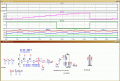
Hi all. I am trying to verify the output for 4 bit SAR logic. So far this is my schematic:

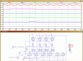
My output plot is showing the expect results of: 1000, 1100, 1110, and 1111 but it doesn't reset after the fourth clock cycle:

These are the values for each component:
 

ericgibbs

Joined Jan 29, 2010
18,873
OK.
The simple method would be add a 5th FF, when clocked it would generate a Clear pulse for all the FF's.
Gate the Clr with the Clk
E
 

ericgibbs

Joined Jan 29, 2010
18,873
hi,
As you know with a SAR into a DAC you require an input voltage that you want to convert to say a 4Bit digital byte.
A comparator is then used to compare the voltage to be converted to the voltage output from the DAC.
Bit3 the MSB of the SAR is set High first and the comparator output 'high or low' determines the next SAR state.

Consider what would happen in your SAR/DAC if the possible input voltage range was 0v to 15v and you had a 7.5V input.???

E

Is this a college or homework project.?

EDIT:
Found a SAR video that may help.
 
Last edited:

Thread Starter

KingPapaya

Joined Oct 28, 2018
14
hi,
As you know with a SAR into a DAC you require an input voltage that you want to convert to say a 4Bit digital byte.
A comparator is then used to compare the voltage to be converted to the voltage output from the DAC.
Bit3 the MSB of the SAR is set High first and the comparator output 'high or low' determines the next SAR state.

Consider what would happen in your SAR/DAC if the possible input voltage range was 0v to 15v and you had a 7.5V input.???

E

Is this a college or homework project.?

EDIT:
Found a SAR video that may help.
Thank you! I am now in the process of recreating the schematic in Cadence. This is part of a project for college.
 

Thread Starter

KingPapaya

Joined Oct 28, 2018
14
After looking over the schematic again and watching the video, I learned the input needs to be a comparator DAC input which I am now having troubles with. I am testing the logic for a 2 bit SAR with voltages ranging from 0-0.3, 0.3-0.6, 0.6-0.9, and 0.9 and above. I am getting the expected results for voltages greater than 0.9 but not for any other voltage. I have also attached my LTSpice schematic. Thanks
 

Attachments

Thread Starter

KingPapaya

Joined Oct 28, 2018
14
I also made an updated 3 bit schematic and tested different voltage inputs. I am also getting the same issue with B2,B1,and B0 not showing accurate results.
 

Attachments

ericgibbs

Joined Jan 29, 2010
18,873
hi KP.
What Vref are you expecting to see when B0,B1,B1 are all High at 1.8V.?
Also what range limit of Ain voltages will be measured.?
I am testing the DAC logic section in isolation, by using fixed 1.8V values for all the B0,1,2 inputs and I get Vref as 1.575V, which looks incorrect.

E
EDIT:
This is the result when testing just the DAC logic, using a counter as an input [ HCT logic levels set to 1.8v]
If you can confirm this is what you expect, let me know and then we can checkout the SAR counter logic.
 

Attachments

Last edited:

Thread Starter

KingPapaya

Joined Oct 28, 2018
14
The Ain voltages and expected outputs are as shown:
Ain>1.75 = 111
Ain< 1.75 & Ain>1.35 = 110
Ain< 1.35 & Ain>1.125 = 101
Ain< 1.125 & Ain>.9 = 100
Ain< .9 & Ain> .675 = 011
Ain< .675 & Ain>.45 = 110
Ain< .45 & Ain>.225 = 001
Ain< .225 = 000

My results on the other hand do not match up:
1.8V = 111
1.7V = 111
1.45 = 111
1.25 = 110
1.00 = 110
.95 = 110
.8 = 011
.5= 011
.3= 010
.2= 010
0 = 000

As for the DAC, I was told by my professor that nothing was wrong with the R2R DAC into the comparator, so the Vref should be as found.
 
Last edited:

ericgibbs

Joined Jan 29, 2010
18,873
hi KP,
Look at my plot image post #14, check that they are what you would expect from that DAC, using that Binary input.???
I used a simple Binary bit step pattern
E

BTW:
With a Vdd for the logic at 1.8V and the loading of the DAC resistors I don't think you will get 1.75V.
As I have posted max I get is 1.57v.
 
Last edited:

Thread Starter

KingPapaya

Joined Oct 28, 2018
14
I will just try doing the 4 bit SAR for values ranging from 0-1.2V instead of 0-1.8V and update with my results later today.
 

Thread Starter

KingPapaya

Joined Oct 28, 2018
14
Based on my 2 bit SAR schematic, the Vref looks as I would expect. As you said about the 1.8V I won't get 1.75V, only a max of 1.57V. So I will used 0-1,2V for my range. I am also really not sure what should happening in this case of Vref for the DAC
 

ericgibbs

Joined Jan 29, 2010
18,873
hi,
You could consider conditioning the Ain to a lower level at the comparator input, so that it matches the Vref steps.
 
Last edited:
Top