The capacitor will charge to 2/3 of the supply pulse, because of the two resistors, so if the pulse is 3v that's 2v, time constant is 1uF x 62k, that is 62mS.
The capacitor woll charge to 2/3 of the supply pulse, because of the two resistors, so if the pulse is 3v that's 2v, time constant is 1uF x 62k, that is 62mS.
The effective charging resistance is the two resistors in parallel - about 40k - which with the 1uF capacitor gives a time constant of 40mS. That is the time to get to roughly 2/3 of the final voltage. The final voltage is roughly 2/3 of the 3.3V supply voltage so it will take roughly 40mS to get to 2/3 x 2/3 x 3.3V oor roughly 1.5V.
The MOSFET will turn on gradually as the voltage rises so the time delay will depend on the particular MOSFET threshold voltage and the load current as a greater gate/source voltage is required for more drain current to flow.
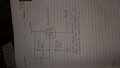
Because it is a very poor schematic.
1. All ground symbols point downward. That thing to the right of R45 is nothing normal in electronics.
2. There is a dangling wire to the left with no indication of what it is for. I assume it connects to a microwave antenna trying to pick up free HBO.
3. In your first post you state that the source is connected to 3.3 V. It is not. The schematic shows clearly that the drain is connected to 3.3 V
4. You should never cross two wires that connect. Stagger them into two T connections with connection dots. When a drawing is printed, copied, scanned, faxed, printed, and copied again, there is no way to tell if a dot on two crossed lines is a connection dot or dirt on a lens.
5. All ground symbols point downward. By general agreement, signal inputs are to the left, signal outputs are to the right, positive supplies are to the top, negative supplies are to the bottom.
The transistor turns on before the full time constant has passed. That is why the delay is less than one TC.
That is a P-MOSFET so with 3.3V connected to the drain as shown, it will conduct through the substrate diode to the source.
The source and drain must be interchanged for the circuit to work at all.
But, even with that change is does not work properly, as shown below with a load resistor and the sudden application of the 3.3V:
Sorry AK, but I did not follow rule #4.
I like neat looking schematics and staggered connections detract from that.
Besides, these days when virtually everything is transmitted as a digital file, I'm not really concerned about it being
That is a P-MOSFET so with 3.3V connected to the drain as shown, it will conduct through the substrate diode to the source.
The source and drain must be interchanged for the circuit to work at all.
There is no way to calculate the exact delay because it is dependent on the details of the transistor's transconductance curves, which vary from part to part and with temperature. Also, as noted above, the output will wander up to 3.3 V, not snap up after the delay. If you pick a point on the transistor's curve and declare that to be when it is "turned on", that gate-source voltage can be used with the R-C exponential equation to calculate when that voltage will be reached. Or, rearranging the equation, you can start with the voltage and a capacitor value and solve for the resistor.
Here's an LTspice simulation of your revised circuit:
It has a simulated turn-on delay of about 20ms for the MOSFET model I used, which has a Vgs(th) of 0.8V.
This is close to the RC time-constant of 41.1ms, where R is the parallel value of R1 and R2, and C=C2.
But as AK noted, that time is dependent on the characteristics of the MOSFET, particularly its threshold voltage Vgs(th), which can have significant unit-to-unit differences, even between MOSFETs of the same type.
If you want an accurate time delay that you can calculate, relatively independent of the MOSFET parameters, then you will need to use a timer circuit to drive the MOSFET, such as a 555, or using an LM339 comparator, which have more accurate switching points.
 Facebook
 Google
 GitHub
 Linkedin