 Facebook
 Google
 GitHub
 Linkedin
Hisense washing machine
- Thread starter haam2924
- Start date

Scroll to continue with content
Hi,
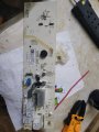
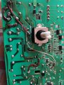
Anybody have image for heisence WM model 7012 like the attached imageView attachment 283416
Attachments
-
 2.8 MB Views: 15
panic mode
- Joined Oct 10, 2011
- 5,067
you need better pictures. need closeup of damaged areas. also it would not hurt to see better the top side. damage is around relays so silkscreen around relays should be better shown.
relays have 12DC coils and one end of the coil is common.
when doing reverse engineering i like to place top and bottom side pictures side by side, then mark on PCb what is on the other side. the solder side pictures are fussy and board needs cleanup. i would use alcohol and cotton swabs, then take better pictures.
this is what it seems to be
panic mode
- Joined Oct 10, 2011
- 5,067

Thanks, I will re attach a clear picture for the damaged areas
Dear panic mode,you need better pictures. need closeup of damaged areas. also it would not hurt to see better the top side. damage is around relays so silkscreen around relays should be better shown.
relays have 12DC coils and one end of the coil is common.
when doing reverse engineering i like to place top and bottom side pictures side by side, then mark on PCb what is on the other side. the solder side pictures are fussy and board needs cleanup. i would use alcohol and cotton swabs, then take better pictures.
this is what it seems to be
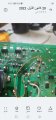
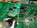
Kindly , I want your help for the lines circled in the attached IMG.
Thanks in advanced,,
Just these lines where are connectedThanks, I will re attach a clear picture for the damaged areas
Attachments
-
 724.6 KB Views: 21
 -
 59.5 KB Views: 20
panic mode
- Joined Oct 10, 2011
- 5,067
not possible with those, you need much better quality pictures
The clear IMG can't be uploaded, I attached more clear pictures hope to help soldering the linesnot possible with those, you need much better quality pictures
Attachments
-
 2.8 MB Views: 9
 -
 2.3 MB Views: 10
 -
 2.3 MB Views: 12
 -
 2.8 MB Views: 11
 -
 3.4 MB Views: 11
 -
 2.5 MB Views: 11
 -
 2.3 MB Views: 10
 -
 3 MB Views: 10
 -
 2.3 MB Views: 12
 -
 3.6 MB Views: 13
panic mode
- Joined Oct 10, 2011
- 5,067
few comments:
when taking closeup photos, use good diffuse lighting to avoid glare. flash light of the phone is less than ideal for this.
images should be sharp with good contrast. while the images are still of poor quality, i think one can deduce what the PCB traces were originally there wires and some pretty scary repair attempt.
pay attention to cuts in the board. they are there to separate high voltage circuits from each other and from low voltage circuit.
in image below they are marked in deep blue.
your repair work around relays must be redone. jumpers you add need to connect proper circuits. also i would make sure that they have insulation or are made of solid wire that is shaped like the PCB track, soldered to track in few places and then covered in hot glue to serve as insulation and ensure no movement.
the yellow tracks are wider and the are high voltage high current (mains). note the cuts in board whenever one of those gets closer to other circuits. CB body is insulation but - it is also convenient surface for contaminants an path for current to creep across which would be unintended.
the orange tracks are low voltage and low current. one of them is a bit wider and goes to coil to each relay (that is the track that goes furthest to the left near bottom left corner). that is the common for the relays. your photos show that you shorted the coil of the K4 relay (pointed by the blue arrow).
i would suggest to use microscope or at least magnifier lamp. at the very least use good magnifier for inspection and cleaning of the board. although photos are smudged and fuzzy, there appear to be tiny solder drops around repair sites.
before the board repair, cause of damage and any external devices that may be destroyed must be replaced too, otherwise board will blow up again. replacing defective components is straight forward. but if programmed IC is damaged, then replacing it is not enough, it would need to be programmed too.
Last edited:
Thanks a lot,few comments:
when taking closeup photos, use good diffuse lighting to avoid glare. flash light of the phone is less than ideal for this.
images should be sharp with good contrast. while the images are still of poor quality, i think one can deduce what the PCB traces were originally there wires and some pretty scary repair attempt.
pay attention to cuts in the board. they are there to separate high voltage circuits from each other and from low voltage circuit.
in image below they are marked in deep blue.
your repair work around relays must be redone. jumpers you add need to connect proper circuits. also i would make sure that they have insulation or are made of solid wire that is shaped like the PCB track, soldered to track in few places and then covered in hot glue to serve as insulation and ensure no movement.
the yellow tracks are wider and the are high voltage high current (mains). note the cuts in board whenever one of those gets closer to other circuits. CB body is insulation but - it is also convenient surface for contaminants an path for current to creep across which would be unintended.
the orange tracks are low voltage and low current. one of them is a bit wider and goes to coil to each relay (that is the track that goes furthest to the left near bottom left corner). that is the common for the relays. your photos show that you shorted the coil of the K4 relay (pointed by the blue arrow).
i would suggest to use microscope or at least magnifier lamp. at the very least use good magnifier for inspection and cleaning of the board. although photos are smudged and fuzzy, there appear to be tiny solder drops around repair sites.
before the board repair, cause of damage and any external devices that may be destroyed must be replaced too, otherwise board will blow up again. replacing defective components is straight forward. but if programmed IC is damaged, then replacing it is not enough, it would need to be programmed too.
View attachment 283808
View attachment 283810
View attachment 283812
I will re check again and feedback.
Hello,few comments:
when taking closeup photos, use good diffuse lighting to avoid glare. flash light of the phone is less than ideal for this.
images should be sharp with good contrast. while the images are still of poor quality, i think one can deduce what the PCB traces were originally there wires and some pretty scary repair attempt.
pay attention to cuts in the board. they are there to separate high voltage circuits from each other and from low voltage circuit.
in image below they are marked in deep blue.
your repair work around relays must be redone. jumpers you add need to connect proper circuits. also i would make sure that they have insulation or are made of solid wire that is shaped like the PCB track, soldered to track in few places and then covered in hot glue to serve as insulation and ensure no movement.
the yellow tracks are wider and the are high voltage high current (mains). note the cuts in board whenever one of those gets closer to other circuits. CB body is insulation but - it is also convenient surface for contaminants an path for current to creep across which would be unintended.
the orange tracks are low voltage and low current. one of them is a bit wider and goes to coil to each relay (that is the track that goes furthest to the left near bottom left corner). that is the common for the relays. your photos show that you shorted the coil of the K4 relay (pointed by the blue arrow).
i would suggest to use microscope or at least magnifier lamp. at the very least use good magnifier for inspection and cleaning of the board. although photos are smudged and fuzzy, there appear to be tiny solder drops around repair sites.
before the board repair, cause of damage and any external devices that may be destroyed must be replaced too, otherwise board will blow up again. replacing defective components is straight forward. but if programmed IC is damaged, then replacing it is not enough, it would need to be programmed too.
View attachment 283808
View attachment 283810
View attachment 283812
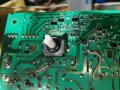
Attached a new photo for the paths soldering.
Is it OK, can I connect the board now to check?
Thanks for the quick response.
Attachments
-
 3.3 MB Views: 9
 -
 3.9 MB Views: 12
panic mode
- Joined Oct 10, 2011
- 5,067
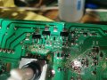
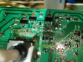
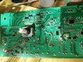
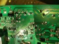
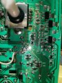
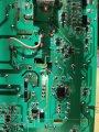
well, i do see some progress. pictures are better. there is no obvious sigh of shorts. it looks like you were scraping off solder mask to check continuity and confirm that repaired traces really connect to intended parts of the circuit.
board is far from clean, i see at least one blob of solder that is large enough to cause short circuit. maintaining circuit integrity by ensuring no debris is floating around is essential. personally i would not tolerate even much smaller contaminants of any kind (conductive or not).

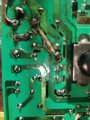
i already mentioned that parts of the circuit connect to mains and that maintaining isolation between circuits is important, hence the board cuts. but your repair ignored clearances. solder blobs and noninsulated parts of wires extend across those board cuts.

and the 'cherry on top' is the burned insulation of wires. moreover wires for low voltage are still routed across board areas that are parts of the mains. i cannot stress enough that this does not meet any standards. we are talking about appliance where dangerous voltages can be present and this is in an environment where steam and condensation are to be expected.
Finally before connecting anything i would recommend to investigate why the board was damaged in the first place. root cause must be eliminated and all damaged components replaced. it is unclear if and what those parts are.
recently i did repair of a dishwasher. the tech wanted to replace the control board which was unavailable (dead time was few months) and it costed 70% of a new appliance. and that is just for the part, not to mention labor and anything else it made it not worth the pain. i am all for repairing things to minimize waste but he did not even bother to try finding what caused board to fail. and it was overheated drain pump with windings melted. so placing new board would not fix anything, new board would just end up in smoke like the original. the solution was to do something he was not ready or capable of - do a real troubleshooting and identify defective part, do the cost analysis. fortunately the price for replacement pump was peanuts and repair still made sense.
based on what i see, the story applies to your case too. repairing PCB traces is a part of the process but ... unless you can find out what caused the damage, you are only mending the symptoms.
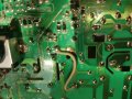
tip:
either your soldering iron is too hot or you keep it in contacts with wire o PCB for far too long.
wires that form jumpers shall not be free to move. they should either be made of solid wire (so they retain the shape) or need to be secured somehow (drop of glue or masking tape) to avoid getting near other circuits, specially when insulation is not rated for handling the voltages or temperature or mechanical wear and tear (due to vibration etc). i used to do repair some some high density circuits using enameled wire. enamel is not designed to endure things like abrasion but such wire can be sufficiently thin to be laid over existing trace (even very thin one). you still want work to look clean and not like something below pigeon hangout so one need to be mindful of amount of glue used. one option is to let the wire touch glue (or nail polish) and when pulled away, only thin layer of glue would be on the wire. placing that wire on the board could make for very little mess and one dried it will be very secure.
one option suitable for wider traces is to form solid wire that match the trace shape then it is laid right on trace and soldered. that way nothing sticks out more than original trace did so there is no risk of issues like clearances between circuits.
for boards with mixed voltages or traces that need long jumper it is recommended to find wire of sufficient gauge and insulation. cut piece that is a bit longer than needed. strip wire ends. tin the wire ends really good (apply flux before tinning) so that solder flows all the way to insulation. then cut the just tinned wire to remove the excess of the wire end. i like to make it no bigger than the size of solder pad. this may mean cutting it close to the insulation. note that insulation cut also need to be clean, no insulation burned or deformed. here is what i mean:

next clean PCB and tin pads where the jumper is to be placed. clean it again. there should be no charred residue or solder blobs or flux or anything else there. now that both board and wire are prepared, bring wire end to the solder pad, and just touch it with soldering iron. this step is very quick the solder from wire and pad should form a very clean joint. and no uninsulated wire would be exposed like here:

and i don't even want to go into wires around relays.
board is far from clean, i see at least one blob of solder that is large enough to cause short circuit. maintaining circuit integrity by ensuring no debris is floating around is essential. personally i would not tolerate even much smaller contaminants of any kind (conductive or not).
i already mentioned that parts of the circuit connect to mains and that maintaining isolation between circuits is important, hence the board cuts. but your repair ignored clearances. solder blobs and noninsulated parts of wires extend across those board cuts.
and the 'cherry on top' is the burned insulation of wires. moreover wires for low voltage are still routed across board areas that are parts of the mains. i cannot stress enough that this does not meet any standards. we are talking about appliance where dangerous voltages can be present and this is in an environment where steam and condensation are to be expected.
Finally before connecting anything i would recommend to investigate why the board was damaged in the first place. root cause must be eliminated and all damaged components replaced. it is unclear if and what those parts are.
recently i did repair of a dishwasher. the tech wanted to replace the control board which was unavailable (dead time was few months) and it costed 70% of a new appliance. and that is just for the part, not to mention labor and anything else it made it not worth the pain. i am all for repairing things to minimize waste but he did not even bother to try finding what caused board to fail. and it was overheated drain pump with windings melted. so placing new board would not fix anything, new board would just end up in smoke like the original. the solution was to do something he was not ready or capable of - do a real troubleshooting and identify defective part, do the cost analysis. fortunately the price for replacement pump was peanuts and repair still made sense.
based on what i see, the story applies to your case too. repairing PCB traces is a part of the process but ... unless you can find out what caused the damage, you are only mending the symptoms.
tip:
either your soldering iron is too hot or you keep it in contacts with wire o PCB for far too long.
wires that form jumpers shall not be free to move. they should either be made of solid wire (so they retain the shape) or need to be secured somehow (drop of glue or masking tape) to avoid getting near other circuits, specially when insulation is not rated for handling the voltages or temperature or mechanical wear and tear (due to vibration etc). i used to do repair some some high density circuits using enameled wire. enamel is not designed to endure things like abrasion but such wire can be sufficiently thin to be laid over existing trace (even very thin one). you still want work to look clean and not like something below pigeon hangout so one need to be mindful of amount of glue used. one option is to let the wire touch glue (or nail polish) and when pulled away, only thin layer of glue would be on the wire. placing that wire on the board could make for very little mess and one dried it will be very secure.
one option suitable for wider traces is to form solid wire that match the trace shape then it is laid right on trace and soldered. that way nothing sticks out more than original trace did so there is no risk of issues like clearances between circuits.
for boards with mixed voltages or traces that need long jumper it is recommended to find wire of sufficient gauge and insulation. cut piece that is a bit longer than needed. strip wire ends. tin the wire ends really good (apply flux before tinning) so that solder flows all the way to insulation. then cut the just tinned wire to remove the excess of the wire end. i like to make it no bigger than the size of solder pad. this may mean cutting it close to the insulation. note that insulation cut also need to be clean, no insulation burned or deformed. here is what i mean:
next clean PCB and tin pads where the jumper is to be placed. clean it again. there should be no charred residue or solder blobs or flux or anything else there. now that both board and wire are prepared, bring wire end to the solder pad, and just touch it with soldering iron. this step is very quick the solder from wire and pad should form a very clean joint. and no uninsulated wire would be exposed like here:
and i don't even want to go into wires around relays.
Thanks,well, i do see some progress. pictures are better. there is no obvious sigh of shorts. it looks like you were scraping off solder mask to check continuity and confirm that repaired traces really connect to intended parts of the circuit.
board is far from clean, i see at least one blob of solder that is large enough to cause short circuit. maintaining circuit integrity by ensuring no debris is floating around is essential. personally i would not tolerate even much smaller contaminants of any kind (conductive or not).
View attachment 283868
i already mentioned that parts of the circuit connect to mains and that maintaining isolation between circuits is important, hence the board cuts. but your repair ignored clearances. solder blobs and noninsulated parts of wires extend across those board cuts.
View attachment 283867
and the 'cherry on top' is the burned insulation of wires. moreover wires for low voltage are still routed across board areas that are parts of the mains. i cannot stress enough that this does not meet any standards. we are talking about appliance where dangerous voltages can be present and this is in an environment where steam and condensation are to be expected.
Finally before connecting anything i would recommend to investigate why the board was damaged in the first place. root cause must be eliminated and all damaged components replaced. it is unclear if and what those parts are.
recently i did repair of a dishwasher. the tech wanted to replace the control board which was unavailable (dead time was few months) and it costed 70% of a new appliance. and that is just for the part, not to mention labor and anything else it made it not worth the pain. i am all for repairing things to minimize waste but he did not even bother to try finding what caused board to fail. and it was overheated drain pump with windings melted. so placing new board would not fix anything, new board would just end up in smoke like the original. the solution was to do something he was not ready or capable of - do a real troubleshooting and identify defective part, do the cost analysis. fortunately the price for replacement pump was peanuts and repair still made sense.
based on what i see, the story applies to your case too. repairing PCB traces is a part of the process but ... unless you can find out what caused the damage, you are only mending the symptoms.
tip:
either your soldering iron is too hot or you keep it in contacts with wire o PCB for far too long.
wires that form jumpers shall not be free to move. they should either be made of solid wire (so they retain the shape) or need to be secured somehow (drop of glue or masking tape) to avoid getting near other circuits, specially when insulation is not rated for handling the voltages or temperature or mechanical wear and tear (due to vibration etc). i used to do repair some some high density circuits using enameled wire. enamel is not designed to endure things like abrasion but such wire can be sufficiently thin to be laid over existing trace (even very thin one). you still want work to look clean and not like something below pigeon hangout so one need to be mindful of amount of glue used. one option is to let the wire touch glue (or nail polish) and when pulled away, only thin layer of glue would be on the wire. placing that wire on the board could make for very little mess and one dried it will be very secure.
one option suitable for wider traces is to form solid wire that match the trace shape then it is laid right on trace and soldered. that way nothing sticks out more than original trace did so there is no risk of issues like clearances between circuits.
for boards with mixed voltages or traces that need long jumper it is recommended to find wire of sufficient gauge and insulation. cut piece that is a bit longer than needed. strip wire ends. tin the wire ends really good (apply flux before tinning) so that solder flows all the way to insulation. then cut the just tinned wire to remove the excess of the wire end. i like to make it no bigger than the size of solder pad. this may mean cutting it close to the insulation. note that insulation cut also need to be clean, no insulation burned or deformed. here is what i mean:
View attachment 283871
next clean PCB and tin pads where the jumper is to be placed. clean it again. there should be no charred residue or solder blobs or flux or anything else there. now that both board and wire are prepared, bring wire end to the solder pad, and just touch it with soldering iron. this step is very quick the solder from wire and pad should form a very clean joint. and no uninsulated wire would be exposed like here:
View attachment 283872
and i don't even want to go into wires around relays.
Is there a schematic diagram for this pcb?
panic mode
- Joined Oct 10, 2011
- 5,067
i am certain that it exists somewhere. it is one of the stage of PCB design. it is another story if this is something easily found on the internet. usually it is not.
Hello,well, i do see some progress. pictures are better. there is no obvious sigh of shorts. it looks like you were scraping off solder mask to check continuity and confirm that repaired traces really connect to intended parts of the circuit.
board is far from clean, i see at least one blob of solder that is large enough to cause short circuit. maintaining circuit integrity by ensuring no debris is floating around is essential. personally i would not tolerate even much smaller contaminants of any kind (conductive or not).
View attachment 283868
i already mentioned that parts of the circuit connect to mains and that maintaining isolation between circuits is important, hence the board cuts. but your repair ignored clearances. solder blobs and noninsulated parts of wires extend across those board cuts.
View attachment 283867
and the 'cherry on top' is the burned insulation of wires. moreover wires for low voltage are still routed across board areas that are parts of the mains. i cannot stress enough that this does not meet any standards. we are talking about appliance where dangerous voltages can be present and this is in an environment where steam and condensation are to be expected.
Finally before connecting anything i would recommend to investigate why the board was damaged in the first place. root cause must be eliminated and all damaged components replaced. it is unclear if and what those parts are.
recently i did repair of a dishwasher. the tech wanted to replace the control board which was unavailable (dead time was few months) and it costed 70% of a new appliance. and that is just for the part, not to mention labor and anything else it made it not worth the pain. i am all for repairing things to minimize waste but he did not even bother to try finding what caused board to fail. and it was overheated drain pump with windings melted. so placing new board would not fix anything, new board would just end up in smoke like the original. the solution was to do something he was not ready or capable of - do a real troubleshooting and identify defective part, do the cost analysis. fortunately the price for replacement pump was peanuts and repair still made sense.
based on what i see, the story applies to your case too. repairing PCB traces is a part of the process but ... unless you can find out what caused the damage, you are only mending the symptoms.
tip:
either your soldering iron is too hot or you keep it in contacts with wire o PCB for far too long.
wires that form jumpers shall not be free to move. they should either be made of solid wire (so they retain the shape) or need to be secured somehow (drop of glue or masking tape) to avoid getting near other circuits, specially when insulation is not rated for handling the voltages or temperature or mechanical wear and tear (due to vibration etc). i used to do repair some some high density circuits using enameled wire. enamel is not designed to endure things like abrasion but such wire can be sufficiently thin to be laid over existing trace (even very thin one). you still want work to look clean and not like something below pigeon hangout so one need to be mindful of amount of glue used. one option is to let the wire touch glue (or nail polish) and when pulled away, only thin layer of glue would be on the wire. placing that wire on the board could make for very little mess and one dried it will be very secure.
one option suitable for wider traces is to form solid wire that match the trace shape then it is laid right on trace and soldered. that way nothing sticks out more than original trace did so there is no risk of issues like clearances between circuits.
for boards with mixed voltages or traces that need long jumper it is recommended to find wire of sufficient gauge and insulation. cut piece that is a bit longer than needed. strip wire ends. tin the wire ends really good (apply flux before tinning) so that solder flows all the way to insulation. then cut the just tinned wire to remove the excess of the wire end. i like to make it no bigger than the size of solder pad. this may mean cutting it close to the insulation. note that insulation cut also need to be clean, no insulation burned or deformed. here is what i mean:
View attachment 283871
next clean PCB and tin pads where the jumper is to be placed. clean it again. there should be no charred residue or solder blobs or flux or anything else there. now that both board and wire are prepared, bring wire end to the solder pad, and just touch it with soldering iron. this step is very quick the solder from wire and pad should form a very clean joint. and no uninsulated wire would be exposed like here:
View attachment 283872
and i don't even want to go into wires around relays.
I just test the board nothing on the screen display.
Any idea for component testing .
The resistor R78 gives about 2k om
It looks like damaged
It looks like damaged
Attachments
-
 70.8 KB Views: 7
Last edited:
panic mode
- Joined Oct 10, 2011
- 5,067
is the board powered? is the supply voltage(s) correct?I just test the board nothing on the screen display.
well... yeah... but each component is different.Any idea for component testing .
Technically with enough of insights, right tools and skill any repair should be possible. but that is a high bar to reach. It does not seem that you have needed skill and what you are working on can be dangerous. also board seem to have suffered extensive damage.
i cannot tell for sure if some of components are just stained or blown since image quality is low. troubleshooting involves many techniques. repairing PCB tracks is important but it is probably the easiest thing one can do.
checking voltages, while leaving all AC side circuits disconnected is probably the best next thing one can try. board does seem to work on 5VDC. then it would be good to see if MCU works: is oscillator running, are buttons responding etc.
personally i would connect that board to separate 5V supply to see if it behaves. and this is safer to work with. all the large white connectors seem to be AC (one is supply, others are output). since the outputs are driven by relays they can be used to power test loads (leds with series resistor).
another thing to consider is how much you plan on investing into repair. new appliance does not cost that much. and if MCU is toast it is not enough to just replace the chip, you would need programmer and actual file to load into the chip.
and yet another option is to check electronics recycling places, they may have bunch of same appliances that are about to be scrapped. getting replacement board from another machine would dramatically improve odds of successful repair.
once the board seem to function, check if the devices that connect to those white connectors are working. if any of them is shorted, it would need to be replaced. alternatively you can power them one at a time and see if they function or blow fuse. only when they are all functional, connect repaired board and put everything together.
there will be things to get familiar with and you will need to do that yourself - for example door switch will need to be closed etc. good luck
OK, it is a good idea to test the board using 5V DC, but I must at the first know the values of the two blows resistors shown in the attached picture.is the board powered? is the supply voltage(s) correct?
well... yeah... but each component is different.
Technically with enough of insights, right tools and skill any repair should be possible. but that is a high bar to reach. It does not seem that you have needed skill and what you are working on can be dangerous. also board seem to have suffered extensive damage.
i cannot tell for sure if some of components are just stained or blown since image quality is low. troubleshooting involves many techniques. repairing PCB tracks is important but it is probably the easiest thing one can do.
checking voltages, while leaving all AC side circuits disconnected is probably the best next thing one can try. board does seem to work on 5VDC. then it would be good to see if MCU works: is oscillator running, are buttons responding etc.
personally i would connect that board to separate 5V supply to see if it behaves. and this is safer to work with. all the large white connectors seem to be AC (one is supply, others are output). since the outputs are driven by relays they can be used to power test loads (leds with series resistor).
another thing to consider is how much you plan on investing into repair. new appliance does not cost that much. and if MCU is toast it is not enough to just replace the chip, you would need programmer and actual file to load into the chip.
and yet another option is to check electronics recycling places, they may have bunch of same appliances that are about to be scrapped. getting replacement board from another machine would dramatically improve odds of successful repair.
once the board seem to function, check if the devices that connect to those white connectors are working. if any of them is shorted, it would need to be replaced. alternatively you can power them one at a time and see if they function or blow fuse. only when they are all functional, connect repaired board and put everything together.
there will be things to get familiar with and you will need to do that yourself - for example door switch will need to be closed etc. good luck
Thanks again for your help.
Attachments
-
 1.6 MB Views: 3
 -
 1.6 MB Views: 3
OK, for the 5vdc where to connect +v terminal?is the board powered? is the supply voltage(s) correct?
well... yeah... but each component is different.
Technically with enough of insights, right tools and skill any repair should be possible. but that is a high bar to reach. It does not seem that you have needed skill and what you are working on can be dangerous. also board seem to have suffered extensive damage.
i cannot tell for sure if some of components are just stained or blown since image quality is low. troubleshooting involves many techniques. repairing PCB tracks is important but it is probably the easiest thing one can do.
checking voltages, while leaving all AC side circuits disconnected is probably the best next thing one can try. board does seem to work on 5VDC. then it would be good to see if MCU works: is oscillator running, are buttons responding etc.
personally i would connect that board to separate 5V supply to see if it behaves. and this is safer to work with. all the large white connectors seem to be AC (one is supply, others are output). since the outputs are driven by relays they can be used to power test loads (leds with series resistor).
another thing to consider is how much you plan on investing into repair. new appliance does not cost that much. and if MCU is toast it is not enough to just replace the chip, you would need programmer and actual file to load into the chip.
and yet another option is to check electronics recycling places, they may have bunch of same appliances that are about to be scrapped. getting replacement board from another machine would dramatically improve odds of successful repair.
once the board seem to function, check if the devices that connect to those white connectors are working. if any of them is shorted, it would need to be replaced. alternatively you can power them one at a time and see if they function or blow fuse. only when they are all functional, connect repaired board and put everything together.
there will be things to get familiar with and you will need to do that yourself - for example door switch will need to be closed etc. good luck


