Help with KiCad - Unconnected Items on DRC

Thread Starter

Dmm

Joined Apr 13, 2015
70
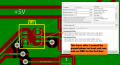
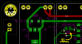
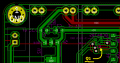
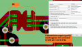
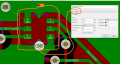
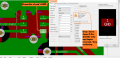
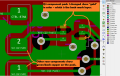
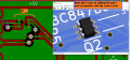
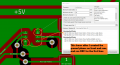
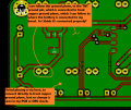
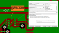
I'm no expert at electronics, but learning a lot, having fun, and I have a few custom PCB designs done and working. My next project, I have the PCB layout completed, created my ground planes on front and back, but I have one component giving me some issues. This component does have 2 ground pads. After creating the ground planes, there is a white line shown from one of the ground pins (pin-4) to the ground plane. When I run DRC it shows two unconnected item issues: Pad 4 to Pad 1 (both are ground pins on the component) and also Pad 4 to zone outline. I tried adding a via, and connecting the two ground pads on the component together, but I can't get rid of this error.

Any suggestions?
 

Attachments

panic mode

Joined Oct 10, 2011
2,715
you should show silkscreen layer so one can confirm which component is Q2.
when creating net classes, i leave GND as a default thin trace. that way reflowing zones is easy. you can also try turning zone view to outline mode to see if the Q2 connection is really made (to KiCAD satisfaction) and not just really close.
 

Thread Starter

Dmm

Joined Apr 13, 2015
70
Yes, I should have shown Q2 better. I've attached a picture (#1) clarifying. It is the 6-pin SMD component with GND at pin 1 and 4.

when creating net classes, i leave GND as a default thin trace
Are you saying my traces are too wide? If you ask why they are that wide, my answer is I don't know. I may have changed defaults a long time ago. I understand wider width can accommodate more current, but I did not size my traces to my currents. Not much running through this component. Maybe 60mA, probably less. I just used what the defaults were (or what I may have changed them to maybe.)

I turned the view to zone view (picture #2) but I'm not sure that helps me any. There is also a zone outline view (picture #3.) I've attached a picture of both.

I also selected the back copper plane, (picture #4) so it is highlighted, and it shows it overlaps the GND pins 1 and 4.

My next thought was to just put a bunch of VIAs connecting ground planes all over the board. That didn't solve anything.

I then clicked on the VIA and went to properties (picture #5) and it does show it to be on GND.

I then clicked on the pad 1 (and also checked pad 4,) and went to properties. This is where something I don't understand may be a cause (picture #6). The component Q2 is showing the pads as green, my back coper layer. But the properties for the pads layer in the drop down shows F.Cu, and a note about he component being flipped and layers reversed. This seems weird to me. I did flip it to be on the back of the board, but why would the drop down show front coper, but the component shows green/back copper? And that note is confusing to me.

I then changed the drop down to F.Cu in the properties for both pad 1 and 4. And now there are no more DRC unconnected errors. The component pad 1 and 4 now show the back mask color. Unlike any other component on the rear where the pads are showing as green/back copper. See picture #7.

I have other components on the rear of the board that I flipped. And they never gave me any issues. So I don't know what I did wrong. Any insights? Suggestions what I should do now? Seems weird just changing the drop down on the properties. I'm not certain the board will be made properly? I just feel like something is wrong and this isn't the proper way to fix it.
 

Attachments

Thread Starter

Dmm

Joined Apr 13, 2015
70
Being curious I attached the 3D view of Q2 to compare. This view is prior to changing the pad properties noted in my previous post. It looks the same as the other rear components. If I do change the pad properties to B.Cu, the 3D view doesn't change, it looks the same.
 

Attachments

panic mode

Joined Oct 10, 2011
2,715
it looks like your net classes and zone setup do not match. yellow arrows are showing minimum clearance based on net class. green arrow is showing minimum clearance as set by zone. if you slightly reduce it, zone islands should connect.
1646409786746.png
 

Thread Starter

Dmm

Joined Apr 13, 2015
70
Thanks for the suggestion of reducing ground plane clearance. I changed it from 0.508 down to 0.20 mm and that solved my DRC errors. I'm still confused why I was getting the error in the first place as when I made the original ground plane they were touching the ground pads. Albeit not a continuous plane, but I thought I could follow a path from one pad to the other, by using vias, but I guess there is something I'm not understanding how it works.

Again, thank you for the suggestion @panic mode , and I'll just roll with it as it worked!
 
Top