Help! H Bridge Circuit using IR2110 and IRF3205

Thread Starter

dknovo

Joined Sep 8, 2014
8
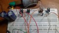
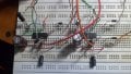
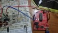
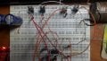
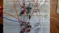
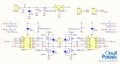
Hi, I'm designing the H bridge circuit uisng IR2110 and IRF3205, but the circuit didn't work. I saw that your circuit works well, (I followed to your diagram circuit). Is anything wrong with my circuit, Can you help me fix st, I don't know how to fix it, my motor DC don't run
Thanks, please help me!
 

Attachments

praondevou

Joined Jul 9, 2011
2,942
Looks right.

Post a picture of your wiring, did you do it on a breadboard?

Also, this circuit doesn't work at 100% duty cycle. You need a PWM on the inputs, I'd say 98% duty cycle would probably work. This is to charge the bootstrap capacitor of the high-sides.
 

Thread Starter

dknovo

Joined Sep 8, 2014
8
Hi, here is my circuit designed on the breadboard. I use MSP430G2553 to produce PWM pulses with PIN1.6 (PWMP) PIN1.0(Direction). As you can see in these pictures, I'm sure everything is corresponding with the Tamid 's diagraml; except for I use diode FR207 instead of uisng UF4007. However the circuit don't work. Please help me, how I can fix with the circuit. :'(
 

Attachments

shortbus

Joined Sep 30, 2009
10,045
The gate drivers and mosfet should be 1"(25mm) or less from each other, the closer the better. Not connected by long wires.
 

Sensacell

Joined Jun 19, 2012
3,451
IMHO - It's a bit of self-abuse trying to build a circuit like this on a solderless breadboard.

Flakey connections can cause the thing to self destruct.
High resistance bus bars create voltage drops- especially when driving high currents.
Lots of parasitic capacitance between clips, terrible high speed performance.

Build this on a real board, with more robust construction techniques, it will make this much less frustrating.
 

Thread Starter

dknovo

Joined Sep 8, 2014
8
Hi, I already removed the resistors connecting between my gate and my source, but the circuit didn't work. How can I fix this circuit now, please help me !!!
Thanks

here is my codes:
//-------------------------------------------------------------------//
#include "msp430g2553.h"
//#include "UART.h"
//#include "Clock.h"

/* The example demonstrates the use of two timers, which
are used to output PWM signals on GPIO pins P1.2 and P2.1 */
unsigned int IncDec_PWM = 1;
void main(void)
{
/*** Watchdog timer and clock Set-Up ***/
WDTCTL = WDTPW + WDTHOLD; // Stop watchdog timer
DCOCTL = 0; // Select lowest DCOx and MODx
BCSCTL1 = CALBC1_1MHZ; // Set range
DCOCTL = CALDCO_1MHZ; // Set DCO step + modulation

/*** GPIO Set-Up ***/

P2DIR |= BIT1;
P2SEL |= BIT1;
P1DIR |= BIT6;
P1SEL |= BIT6;

P1DIR |= BIT0;

/* Timer0_A Set-Up */
TA0CCR0 = 1000; //PWM Period
TA0CCTL1 = OUTMOD_7; //TA0CCR1 output mode = reset/set
TA0CCR1 = 1; //TA0CCR1 PWM duty cycle
TA0CTL = TASSEL_2 + MC_1; //SMCLK, Up Mode (Counts to TA0CCR0)


/* Timer1_A Set-Up */
TA1CCR0 = 4000; //Counter value
TA1CCTL0 = CCIE; //Enable Timer1_A interrupts
TA1CTL = TASSEL_2 + MC_1;

_BIS_SR(LPM0_bits + GIE);
}

#pragma vector=TIMER1_A0_VECTOR
__interrupt void Timer1_A0 (void){

TA0CCR1 += IncDec_PWM *2;
if(TA0CCR1 > 998 || TA0CCR1 < 2)
{
IncDec_PWM = -IncDec_PWM;
P1OUT = BIT0;
}
}
 

Attachments

shortbus

Joined Sep 30, 2009
10,045
I'd suggest you download and read IRF application note AN-978. Your breaking so many of the rules in that app note I can't begin to describe them. A big one from the top of page #6,
" Therefore it is always better to use a non-electrolytic capacitor if possible." Also read section #6, starting on page #11. And see if you have followed those guidelines. IRF and other companies spend a lot of money figuring this stuff out, take advantage of their knowledge!

AN-978 here - http://www.google.com/url?sa=t&rct=j&q=&esrc=s&source=web&cd=1&ved=0CB8QFjAA&url=http://www.irf.com/technical-info/appnotes/an-978.pdf&ei=_hkUVYn_JMGqoQTyl4GIDw&usg=AFQjCNHRAOvF_G6P5rcv6Kyd_fjU1B__Rg
 

Sensacell

Joined Jun 19, 2012
3,451
What you must understand is that modern high-performance electronic parts makes demands on circuit layout that you are not taking into account.
The circuit board is not just a bunch of wires connecting point A to B, but an integral part of the electrical design.

To get the FET's to switch at nanosecond speeds, the gate drivers need to push heavy currents in and out of the mosfet gate, this is where the casual approach fails.
The solderless breadboard is hopeless in terms of it's electrical performance at these speeds and current levels.
These fast current spikes require careful layout consideration. Read the app notes about layout, bypassing capacitors and lead lengths, etc.
 

praondevou

Joined Jul 9, 2011
2,942
He says, his circuit does not work at all. While I agree layout is very important he should be able to get something at the load terminals. He apparently isn't even able to blow up the circuit, so his main problem does not seem to be related to gate ringing, shot-throughs etc.

@OP, you need an oscilloscope to troubleshoot your circuit.
 

praondevou

Joined Jul 9, 2011
2,942
From Arduino to the breadboard, is there a reference connection? In other words, ground of Arduino is connected to GND of breadboard?

EDIT:
Just from looking at your photos it's hard to impossible to find the error. You should clean it up. Use short direct wires. This will enable us to troubleshoot your circuit.

You would start by verifying the following:
- power supply IR2110
- SD pin IR2110
- Bus voltage (main bridge voltage)
- input pulses going to the IR2110
- output pulses from IR2110
- bootstrap voltages

You will find the problem within minutes with the help of an oscilloscope.

All other recommendations that were posted regarding the layout are equally important. Otherwise you will blow up the circuit in no-time once you put real load on it.
 
Last edited:
Top