Ground plane / power plane

Thread Starter

hrs

Joined Jun 13, 2014
520
Hi,

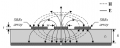
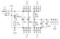
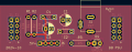
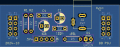
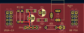
A while ago I made a power adapter for breadboards. It is as per attached images. It's a simple circuit so in this case it probably doesn't matter much, but ...

In principle, would it have been better to have routed power with traces, made a copper pour and via stitched that pour to the ground plane?

On the one hand, with a power and ground plane you get coupling across the entire board though it's probably nothing compared to the caps. On the other hand the electric fields in any signal traces will now couple with the ground plane underneath and the power plane right next to it (in-plane) thus you get a capacitive divider across the signal trace which is bad. With a pour stitched to ground signals only couple to ground.

Does the magnetic fields couple into anything?

edit: Aargh. The image names ground is power. The image named power is ground.
 

Attachments

Last edited:

Thread Starter

hrs

Joined Jun 13, 2014
520
I don't buy that.
Which part exactly?
What would you call the common plane in this case? I'd call it ground.
Would you agree that having a capacitive divider across a signal is bad? Vref in this case, but in general?
How strong is the coupling to a plane below vs in-plane coupling?
Does the magnetic field couple into anything?

For the sake of this discussion let's say signals not much faster that 1MHz.
 

MrChips

Joined Oct 2, 2009
34,628
You have two power planes:
1) V+ (RED)
2) V- (BLUE)

C1 and C2 are low AC impedance paths that connect the two planes. That is good.

Vref has a low AC impedance connection to V- via C3 and C4. That is also good.

I don't see anything wrong with your layout.
The only thing I would quibble over, is the distance between the capacitors and what they are supposed to protect.
C1 should be on the input at J1.
C2 should be at J3 and J4.

Similarly, C3 should be at R1 and R2.
C4 should be at J6.

You need to pay attention to the length of PCB traces. Every trace is an inductor. C4 is connected by a trace that is too long.
For the intended application of this board, you don't need C2 and C4. They should go on the device that is being powered.
I can also make the argument that you don't need the capacitors. Again, they go on the device board.
 

nsaspook

Joined Aug 27, 2009
16,250
If you really want to know what's happening, you need the correct equipment to measure it. It's too expensive to get a 2MHz to 6GHz EM field probe for a O-scope.

1747244790931.png
1747244829797.png
Field probes testing the LCD for emissions.

1747244874545.png
1747244899837.png
(E probe) Looking at the E-field fundamental frequency 16 MHz energy on a trace from the clock OSC to the uC.

1747245018684.png
1747245057009.png
1747245275385.png
(M probe) Looking at B-field harmonic energy (from signal edges) from the clock OSC with a 200+ MHz ring from the circuit trace and components reactance.
 
Last edited:

Thread Starter

hrs

Joined Jun 13, 2014
520
If you really want to know what's happening, you need the correct equipment to measure it. It's too expensive [snip]
Yes, expensive and I wouldn't really know how to make good use of it.

I'm just trying to get my head around the Rick Hartley school of thought. That is signal integrity on the one hand and EMI on the other. My noob stuff probably doesn't warrent EMI consideration too much.

After posting that video snippet I wondered, if you have a power(VCC) and a ground plane pour, wouldn't a sliver of VCC between signal traces also be bad? So as a default on 2 layer boards have ground plane pour and on the other only power and signal traces where needed or is ground pour and power pour generally fine? Or there is no general case and it depends ... maybe some day I'll get it.
 

crutschow

Joined Mar 14, 2008
38,316
The purpose of a ground or power plane is to (ideally) eliminate any significant inductive or resistive impedance across the plane so that all points on the plane are at the same potential.
So a plane is almost always better than a trace to provide power and ground.
 

nsaspook

Joined Aug 27, 2009
16,250
Yes, expensive and I wouldn't really know how to make good use of it.

I'm just trying to get my head around the Rick Hartley school of thought. That is signal integrity on the one hand and EMI on the other. My noob stuff probably doesn't warrent EMI consideration too much.

After posting that video snippet I wondered, if you have a power(VCC) and a ground plane pour, wouldn't a sliver of VCC between signal traces also be bad? So as a default on 2 layer boards have ground plane pour and on the other only power and signal traces where needed or is ground pour and power pour generally fine? Or there is no general case and it depends ... maybe some day I'll get it.
Not outrageous: https://www.amazon.com/Tekbox-TBPS01-Near-Field-Wideband-Amplifier/dp/B00OD57L4G/ref=mp_s_a_1_5?crid=16XC1DGSPV97R&dib=eyJ2IjoiMSJ9.hbLK_aIJFVE6PTJ1mHe9qSgbRbx9LtvXqrhBcZpouc2pddP3PLrcaSz2GIaCz1u8NBLPt2QP0QubNU0hH6V9NTkm4agZRS3STUPPP0RepICJeMO2sSnhEB1ut8LKVYaEQL1cVRelMgEd5XEsNbb0etUTc5tGjCZRxy6OT6QPUYwLiDpd7Wl7q6jiM5rjrzE4jmpDTim2HSkYz5s1XPl3Eg.u3Aa3S14UzOYXebEv45p3Mzl5-pnYi5OGxjh_bGYBUM&dib_tag=se&keywords=emc+emi+near+field+probe+and+amplifier&qid=1747258562&sprefix=emi+prob,aps,221&sr=8-5

The signal energy flows between the traces so just laying down grounds at random moves the energy to the surfaces, not under the traces like you want in most cases outside of matching transmission lines to things like complex antenna impedance loads.

https://youtube.com/shorts/D5dhRgeZYHA?si=wXPGhueh9ShTvzfl
 
Last edited:

BobTPH

Joined Jun 5, 2013
11,463
Seeing as there are no signals of any frequency on your board, I wonder what it is you are worried about? I power my breadboards from two ~1m wires to a lab supply. And I have run microcontrollers with 8MHz clocks on them, though no external signals were anywhere near that.

Surprisingly, I also built a ~100MHz single transistor FM transmitter on a standard solderless breadboard, which, pretty much any EE would say is impossible. It must have worked because I didn’t know any better.
 

nsaspook

Joined Aug 27, 2009
16,250
Seeing as there are no signals of any frequency on your board, I wonder what it is you are worried about? I power my breadboards from two ~1m wires to a lab supply. And I have run microcontrollers with 8MHz clocks on them, though no external signals were anywhere near that.

Surprisingly, I also built a ~100MHz single transistor FM transmitter on a standard solderless breadboard, which, pretty much any EE would say is impossible. It must have worked because I didn’t know any better.
Not impossible, just not very Smart.

Engineering is about repeatability and reliability. Giving advice on how make it work with a very high probability, with a high degree of variation of build variations, from a crappy breadboard to a multi-layer well designed PCB.

Playing Russia roulette with circuits is not good engineering.

The hope is to learn good circuit construction habits before they become critical to success, so when there is a task that needs attention to such details, you don't look like a fool.
 
Last edited:
Top