 Facebook
 Google
 GitHub
 Linkedin
So, one thing I need to figure out is properly interfacing a 68HC11 MPU (Motorola) to a 8279 display controller (Intel).
The Motorola 68xx architecture makes use of a single R/~W line, while the Intel architecture calls for separate ~RD and ~WR lines.
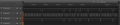
The attachment shows the waveforms as measured in the piece of equipment I'm been dinking around with, and I want to see if this is what I'm supposed to have - in other words, whether the step of OR-ing the signals with the system clock is mandatory.
The first waveform is the R/~W signal as generated by the 68HC11.
The second is the ~RD signal; the R/~W signal is inverted then OR-ed with the system clock to generate this signal.
The third is the ~WR signal, which is just the R/~W signal OR-ed with the system clock.
The Motorola 68xx architecture makes use of a single R/~W line, while the Intel architecture calls for separate ~RD and ~WR lines.
The attachment shows the waveforms as measured in the piece of equipment I'm been dinking around with, and I want to see if this is what I'm supposed to have - in other words, whether the step of OR-ing the signals with the system clock is mandatory.
The first waveform is the R/~W signal as generated by the 68HC11.
The second is the ~RD signal; the R/~W signal is inverted then OR-ed with the system clock to generate this signal.
The third is the ~WR signal, which is just the R/~W signal OR-ed with the system clock.
Attachments
-
 28 KB Views: 7


