***Gain of Differential Amplifier Keeps changing***

Thread Starter

artmaster547

Joined Jan 6, 2016
409
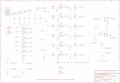
Hi All I have designned a PCB that compares voltages of cells, I have now created the PCB and I am currently testing it, I have applied a fixed DC voltage across the inputs: i.e. c1- and c1+ and I am finding that when I change the input voltage and measure the output voltage of the differential amplifiers the gain keeps changing, I do not fully understand why because when running simulations everything seemed to function fine any help would be greatly appreciated. The resistors have a tolerance of ±1%. And the op-amp that is being used: STMicro MPN: MC33174

Thanks
Art
 

Attachments

Last edited:

kubeek

Joined Sep 20, 2005
5,796
The main problem with this setup is the CMRR aka common mode rejection ration of each differential amplifier. Since the four resistors that set the gain are not exactly the same, the output will not only depend on the difference voltage on the inputs, but also on the offset of those inputs above ground. Using 1% or even 0.1% or trimming manually will probably be necessary to get rid of this.

Another option is to use a voltage to current converter, but that will probably not work very well for low-voltage cells.
 

Kjeldgaard

Joined Apr 7, 2016
476
What are the tolerances of the resistors?

And I would like to see some figures on changes in the differential amplifier's output relative to the input voltages?
 

Thread Starter

artmaster547

Joined Jan 6, 2016
409
What are the tolerances of the resistors?

And I would like to see some figures on changes in the differential amplifier's output relative to the input voltages?
If you look at the last three columns I just applied voltages of 1-5V and measured voltages at the input and output of the differential amplifiers
 

Attachments

Thread Starter

artmaster547

Joined Jan 6, 2016
409
The main problem with this setup is the CMRR aka common mode rejection ration of each differential amplifier. Since the four resistors that set the gain are not exactly the same, the output will not only depend on the difference voltage on the inputs, but also on the offset of those inputs above ground. Using 1% or even 0.1% or trimming manually will probably be necessary to get rid of this.

Another option is to use a voltage to current converter, but that will probably not work very well for low-voltage cells.
The resistors I have used are 1%, does my choice of op-amp have any effect? And is the CMRR responsible for the changes in gain?
 

Thread Starter

artmaster547

Joined Jan 6, 2016
409
What are the tolerances of the resistors?

And I would like to see some figures on changes in the differential amplifier's output relative to the input voltages?
In theory the gain should just be constant from what I can see, but as you see just by changing which op-amp I am looking at there is change in gain and also there is a fluctuation in the gain calcualted
 

kubeek

Joined Sep 20, 2005
5,796
looking at your data, I don´t think you are calculating it correctly, or I am missing something.
First of all, you have 6 input pins, but you have only 5 voltages in the first column (but should be 6).
Then after Vin differential column you have straight Vout differential, but that does not make sense. Vout diff #1 should be calculated from voltages in row 1 and row 2, not from just that one row and with five input voltages you should come up with onlz four Vout differental.
 

Thread Starter

artmaster547

Joined Jan 6, 2016
409
looking at your data, I don´t think you are calculating it correctly, or I am missing something.
First of all, you have 6 input pins, but you have only 5 voltages in the first column (but should be 6).
Then after Vin differential column you have straight Vout differential, but that does not make sense. Vout diff #1 should be calculated from voltages in row 1 and row 2, not from just that one row and with five input voltages you should come up with onlz four Vout differental.
oh no sorry I was just looking at one differential amplifier setup basically between c1- and c1+ these are potential divided then buffered as inputs to the differential amplifier. The first coloum is basically the voltage of say C1+ ad c1- is considered GND from the supply I used.
 

Thread Starter

artmaster547

Joined Jan 6, 2016
409
looking at your data, I don´t think you are calculating it correctly, or I am missing something.
First of all, you have 6 input pins, but you have only 5 voltages in the first column (but should be 6).
Then after Vin differential column you have straight Vout differential, but that does not make sense. Vout diff #1 should be calculated from voltages in row 1 and row 2, not from just that one row and with five input voltages you should come up with onlz four Vout differental.
I'm only talking about the last three columns btw in reference to the Differential amplifier, would you like me to include the LTSpice simulation I created perhaps that would be more useful:
 

Thread Starter

artmaster547

Joined Jan 6, 2016
409
looking at your data, I don´t think you are calculating it correctly, or I am missing something.
First of all, you have 6 input pins, but you have only 5 voltages in the first column (but should be 6).
Then after Vin differential column you have straight Vout differential, but that does not make sense. Vout diff #1 should be calculated from voltages in row 1 and row 2, not from just that one row and with five input voltages you should come up with onlz four Vout differental.
 

Attachments

Thread Starter

artmaster547

Joined Jan 6, 2016
409
looking at your data, I don´t think you are calculating it correctly, or I am missing something.
First of all, you have 6 input pins, but you have only 5 voltages in the first column (but should be 6).
Then after Vin differential column you have straight Vout differential, but that does not make sense. Vout diff #1 should be calculated from voltages in row 1 and row 2, not from just that one row and with five input voltages you should come up with onlz four Vout differental.
I remade the table to make it clearer what I had layed out before was incorrect the following are the correct results I collected:
 

Attachments

crutschow

Joined Mar 14, 2008
38,323
In theory the gain should just be constant from what I can see,
Welcome to the non-virtual (real) world. :rolleyes:
For ideal resistors and amplifiers, as in your simulation, the output voltage (and apparent gain) would be constant with a change in common-mode voltage
In a real circuit, no.
Here's the simulation of one of your differential stages with worst-case 1% resistor values, a 500mV constant differential signal and the common-mode voltage ramping from 1V to 4V.
As you can see, the output voltage (middle trance), and the apparent gain (bottom trace) change with the common-mode voltage, V_cm [V(in2)], but that's just the common-mode voltage gain, which is no longer zero due to the tolerance of the resistor values.

So to minimize that, you either need to use tighter tolerance resistors, or go to a difference amp, where the internal resistor values are laser trimmed to tight ratio tolerances.

upload_2017-2-17_11-3-1.png
 

Thread Starter

artmaster547

Joined Jan 6, 2016
409
Welcome to the non-virtual (real) world. :rolleyes:
For ideal resistors and amplifiers, as in your simulation, the output voltage (and apparent gain) would be constant with a change in common-mode voltage
In a real circuit, no.
Here's the simulation of one of your differential stages with worst-case 1% resistor values, a 500mV constant differential signal and the common-mode voltage ramping from 1V to 4V.
As you can see, the output voltage (middle trance), and the apparent gain (bottom trace) change with the common-mode voltage, V_cm [V(in2)], but that's just the common-mode voltage gain, which is no longer zero due to the tolerance of the resistor values.

So to minimize that, you either need to use tighter tolerance resistors, or go to a difference amp, where the internal resistor values are laser trimmed to tight ratio tolerances.

View attachment 120747
thank you so much! This is my first time designning something for the real world, thank you for carrying out the simulations it's super helpful and something I will bare in mind in the future when designning for such applications. May I ask do you have any suggestions of how to select a difference amp? Did you have any mind that will work for my application? Kind Regards Art
 

crutschow

Joined Mar 14, 2008
38,323
do you have any suggestions of how to select a difference amp? Did you have any mind that will work for my application?
On second thought, an instrumentation amp should work better since many (but not all) already have the NI buffer amps for a high input impedance at the input, so you can eliminate the ones you have.
Simulation of a typical such amp (LT1167) is below.
The gain is easily set by just one external resistor, Rg.
Note the constant output amplitude (and constant apparent gain) with change in common-mode voltage [V(in2)].
(The glitches in the gain are just due to a discontinuity in the gain calculation at the sinewave zero crossing).

There are many such instrumentation amps available from various manufacturers so just select one that best fits your cost and performance requirements.
Here are some less expensive ones, for example.
Any questions on that, let us know. :)

upload_2017-2-18_9-4-15.png
 
Last edited:
Top