Full H Bridge - output changes when piezo disc load is connected

Thread Starter

chendhir kumar

Joined Oct 13, 2017
2
Hi, I'm new to power electronics and have very little knowledge in that..
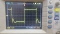
I have rigged up a full H bridge using 2 pairs of N & P channel mosfets. The wave form at no load and full load are attached. kindly advice me where i'm going wrong as when you see the no load waveform, a hump is found soon after the switching of mosfets.

Also at full load, the square wave almost becomes a saw tooth wave with a ramp in voltage after the switching happens.

kindly note that in the schematic, (NI) mentioned components are not installed.

MOD: Rotated and lightened the sch.E
 

Attachments

Last edited by a moderator:

crutschow

Joined Mar 14, 2008
34,472
What is the capacitance of the piezo load?

Turning the upper and lower MOSFETs on and off with the same signal will generate larger feedthrough currents when they are both on during the signal transition.
You need a gate driver circuit (available as an IC) that will generate separate non-overlap drive signals to each MOSFET so that the two MOSFETS are never on at the same time.

Why do you have resistors going from the MOSFET sources and drains to the gates?

Where did you get that schematic?
 

ericgibbs

Joined Jan 29, 2010
18,879
hi Carl,
The 'E' is a Euro 'thing', personally I prefer the familiar 'R'.
E

web clip:
What does E mean in resistors?
In some circuit diagrams, a value such as 8 or 120 represents a resistance in ohms. Another common practice is to use the letter E for resistance in ohms. The letter R can also be used. For example, 120E (120R) stands for 120 Ω, 1E2 stands for 1R2 etc.
 

Thread Starter

chendhir kumar

Joined Oct 13, 2017
2
What is the capacitance of the piezo load?

Turning the upper and lower MOSFETs on and off with the same signal will generate larger feedthrough currents when they are both on during the signal transition.
You need a gate driver circuit (available as an IC) that will generate separate non-overlap drive signals to each MOSFET so that the two MOSFETS are never on at the same time.

Why do you have resistors going from the MOSFET sources and drains to the gates?

Where did you get that schematic?
The
resistors going from the MOSFET sources and drains to the gates are not installed components. Also the "E"
stands for R which i found explained in the following posts.

The Components mentioned in schematic marked as (NI) are not installed. As you have advised, i will change the schematic to drive each gate of MOSFET with a dedicated IO pin from my micro and ensure a small dead time (around 400nS between transitions ).

My next concern is about the output when 12 piezo disc connected.
The capacitance of one piezo is 65nF . 12 piezo Connected in parallel. So i believe the cap of 12 piezo should come to 780nF. But when i check the capacitance using LCR meter ,the capacitance reads to 1.4UF.

Kindly suggest how to over come the waveform change when piezo's are connected.
 

Attachments

Top