Facebook
 Google
 GitHub
 Linkedin
Hi everyone,
I would greatly value any input on a load cell conditioning circuit that I designed for a livestock scale. I work for a small company as the sole electronic engineer, and being a recent graduate with no senior electronic engineers to learn from, am still inexperienced and cannot get technical input from superiors. I cannot divulge on the forum too many details of my design, at request of my employer, but will try to give sufficient information for informed advice.
A brief overview of the circuit:
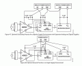
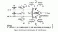
Four load cells, excited with the same 5V supply rails used to supply the rest of the analogue circuitry, are each fed to the input of an INA332 instrumentation amplifier. The IA is configured with external resistors to have a gain of 905 V/V, which is within, but near the maximum of the rated gain range given in the datasheet (rated maximum is 1000 V/V). The REF input is fed from a MCP6022 opamp buffer, which in turn is fed by a resistive voltage divider and first-order low pass filter. The REF voltage is 50mV (as I am only interested positive voltages from the load cells). The IA is then fed to another passive, first-order low pass filter and then to an input of a CD4051 multiplexer. This is repeated for each of the four load cells, with four of the MUX inputs being used. The second opamp in the MCP6022 chip is then used to buffer the output of the MUX (improving the voltage loading factor between the MUX and the ADC). The buffer is then fed to the ADC of a STM32F4 microcontroller through a 2m cable. The STM32 sets the control pins of the MUX and then polls for an ADC reading, cycling through the four channels continuously and performing running averaging.
The load cells are 2T, shear-beam load cells, which are much more competitively priced than other load cells that I could source here in South Africa. I am not using their full range (hence the high IA gain) and have designed for a total capacity of 2T.
Some relevant given specs of the load cells:
- Sensitivity: 2.0000±0.002mV/V
- Total error: ±0.02%F.S
- Creep (30 minutes): ±0.02%F.S.
- Recommended voltage: 5V~12V
- Zero balance: ±1%F.S.
- Temperature effect on load: ±0.02%F.S/10℃
- Temperature effect on zero: ±0.02%F.S/10℃
My problem:
With four load cells connected and sitting on the bench with their casings grounded I have stable readings with little fluctuation, but with the the load cells installed in steel weigh beams or with the casings ungrounded, I experience fluctuations in the voltage read by the ADC. The voltages output for each channel seem, within a matter of seconds, to drift by 50 LSBs of the MCU's 12-bit ADC (~ 40.3 mV). The casings of the load cells seem to be isolated from the internal Wheatstone bridge and therefore are not grounded unless I ground them externally. When the load cells are installed in the weigh beams, they also seem to interfere with one another. For instance, if I disconnect or apply shear force to just one cell, the readings of all four channels vary (not so if they are not installed in the steel weigh beams).
My questions:
1. Should I be grounding the weigh beams (and thereby the load cell casings), and if so, how should I be doing so? Could this pose a risk of ground loops? I am uncertain, as I assume that the casings were intentionally not grounded by the manufacturer but grounding them seems to stabilize the readings. This may be a very trivial question, but I admit my ignorance, and am a little confused.
2. Am I too audacious to use a single amplifier stage with a gain of 905 V/V? I believe that my gain/phase margins are sufficient, given the very low frequency passband.
3. Is it generally unwise to use high-capacity load cells at only a quarter of their capacity with high-gain amplification as opposed to using lower-capacity load cells? Once again, my only reason for using the 2T load cells is cost, and if it is unwise then I should rather redesign for lower-capacity load cells.
Thank you in advance for your time and willingness to consider my problem and offer advice. Any input or pointers, however brief, will be appreciated immensely. I can share more details on the design privately if need be.
I would greatly value any input on a load cell conditioning circuit that I designed for a livestock scale. I work for a small company as the sole electronic engineer, and being a recent graduate with no senior electronic engineers to learn from, am still inexperienced and cannot get technical input from superiors. I cannot divulge on the forum too many details of my design, at request of my employer, but will try to give sufficient information for informed advice.
A brief overview of the circuit:
Four load cells, excited with the same 5V supply rails used to supply the rest of the analogue circuitry, are each fed to the input of an INA332 instrumentation amplifier. The IA is configured with external resistors to have a gain of 905 V/V, which is within, but near the maximum of the rated gain range given in the datasheet (rated maximum is 1000 V/V). The REF input is fed from a MCP6022 opamp buffer, which in turn is fed by a resistive voltage divider and first-order low pass filter. The REF voltage is 50mV (as I am only interested positive voltages from the load cells). The IA is then fed to another passive, first-order low pass filter and then to an input of a CD4051 multiplexer. This is repeated for each of the four load cells, with four of the MUX inputs being used. The second opamp in the MCP6022 chip is then used to buffer the output of the MUX (improving the voltage loading factor between the MUX and the ADC). The buffer is then fed to the ADC of a STM32F4 microcontroller through a 2m cable. The STM32 sets the control pins of the MUX and then polls for an ADC reading, cycling through the four channels continuously and performing running averaging.
The load cells are 2T, shear-beam load cells, which are much more competitively priced than other load cells that I could source here in South Africa. I am not using their full range (hence the high IA gain) and have designed for a total capacity of 2T.
Some relevant given specs of the load cells:
- Sensitivity: 2.0000±0.002mV/V
- Total error: ±0.02%F.S
- Creep (30 minutes): ±0.02%F.S.
- Recommended voltage: 5V~12V
- Zero balance: ±1%F.S.
- Temperature effect on load: ±0.02%F.S/10℃
- Temperature effect on zero: ±0.02%F.S/10℃
My problem:
With four load cells connected and sitting on the bench with their casings grounded I have stable readings with little fluctuation, but with the the load cells installed in steel weigh beams or with the casings ungrounded, I experience fluctuations in the voltage read by the ADC. The voltages output for each channel seem, within a matter of seconds, to drift by 50 LSBs of the MCU's 12-bit ADC (~ 40.3 mV). The casings of the load cells seem to be isolated from the internal Wheatstone bridge and therefore are not grounded unless I ground them externally. When the load cells are installed in the weigh beams, they also seem to interfere with one another. For instance, if I disconnect or apply shear force to just one cell, the readings of all four channels vary (not so if they are not installed in the steel weigh beams).
My questions:
1. Should I be grounding the weigh beams (and thereby the load cell casings), and if so, how should I be doing so? Could this pose a risk of ground loops? I am uncertain, as I assume that the casings were intentionally not grounded by the manufacturer but grounding them seems to stabilize the readings. This may be a very trivial question, but I admit my ignorance, and am a little confused.
2. Am I too audacious to use a single amplifier stage with a gain of 905 V/V? I believe that my gain/phase margins are sufficient, given the very low frequency passband.
3. Is it generally unwise to use high-capacity load cells at only a quarter of their capacity with high-gain amplification as opposed to using lower-capacity load cells? Once again, my only reason for using the 2T load cells is cost, and if it is unwise then I should rather redesign for lower-capacity load cells.
Thank you in advance for your time and willingness to consider my problem and offer advice. Any input or pointers, however brief, will be appreciated immensely. I can share more details on the design privately if need be.
.jpeg")