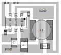
First buck convertor - please give me feedback

dl324

Joined Mar 30, 2015
16,918
  1. Too many unnecessary wire jogs.
  2. Too many trace widths.
  3. Would be more aesthetically pleasing if the components were placed in the same orientation.
  4. Can't see the connections on many of the components (D1, C1, C2, R1, R2, R3, ...).
 

Thread Starter

Wolframore

Joined Jan 21, 2019
2,610
Is this easier to see? I've tried to stick to their recommendations for short traces where required... V in will be at the anode of D1 (I figure voltage drop won't hurt in this case) and Vout is junction of C2 and L1.... the long leg on the right go back to feedback loop... There's also a full ground plane under this board.

upload_2019-7-19_12-43-5.png

here's the layout per the datasheet...

upload_2019-7-19_12-47-29.png
 
Last edited:

MrAl

Joined Jun 17, 2014
11,474
Hi,

The buck circuit is the simplest of all the switchers.
The output voltage is proportional to the duty cycle.
The inductor and capacitor filter the switch pulses.
The inductor provides for a true power conversion not just a voltage step down.
 

Thread Starter

Wolframore

Joined Jan 21, 2019
2,610
The switching frequency is 1.4 MHz it's good that's its inaudible.. , I plan to use this with microcontrollers, audio and 2.4 Ghz transceiver. How do I minimize EMI and keep noise away from other circuits... is it distance, shielding... filters? I'm not concerned about the fundamental so much but it can cause summation and difference frequencies, I'm sure...

Also how is the Vin/Current vs Vout/Current calulated... is it a direct conversion minus the efficiency factor?
 
Last edited:

MrAl

Joined Jun 17, 2014
11,474
Start with a ground plane.

There are shielding materials.
The old Timex Sinclair used a metal plating on the inside of the plastic case connected to ground with a spring loaded contact.
 

Thread Starter

Wolframore

Joined Jan 21, 2019
2,610
I worked with microwave radio and metal shielding is best was wondering what my other options are... metal shielding can get pricey to do correctly.

Exploring options for future:
being conscious of ground loops
ferrite beads
inductor coupling
additional supply capacitors...
1/4 wave antenna at ground... not practical haha.

Am I missing any?

as to reducing RF transmission and reducing antenna area... where should I be focusing?

Here's a novel solution... isolate the switching supply and output about 7V then use a 7805 for quiet power...
 

TeeKay6

Joined Apr 20, 2019
573
Is this easier to see? I've tried to stick to their recommendations for short traces where required... V in will be at the anode of D1 (I figure voltage drop won't hurt in this case) and Vout is junction of C2 and L1.... the long leg on the right go back to feedback loop... There's also a full ground plane under this board.

View attachment 182063

here's the layout per the datasheet...

View attachment 182064
@Wolframore
Viewing your layout post#3.
Some general guidelines:
*Keep all traces as short as possible; this may require trying numerous different attempts at layout before you achieve the best you can do. Using a manufacturer-recommended layout is a good start, but that does not mean the layout cannot be improved. Viewing the layout in your post#3, I somewhat doubt that this is the best achievable layout. However, it may well be a very acceptable layout! I refrain from specific comments.

*Keep all conductive loops (whether created by PCB traces or components) as small as possible, enclosing the least area possible. Loops resonate, both efficiently emitting and receiving high frequency signals.

*Wide traces have lower inductance (and thus impedance) than narrow traces; wide traces can also carry more current without overheating. To keep the layout as compact as possible, use trace widths appropriate for their function and the current they must carry. It is not unusual to use traces varying in width from 0.008" up to 0.25 inches (or more) in one layout. Nor does a trace have to a constant width; it is okay to "neck down" a wide trace to get through a tight space yet have little effect on the value of the full trace.

*There is dispute as to the efficacy of this, but some people claim that trace corners should never be sharp, but rather rounded.

*Bear in mind that the PCB material itself is the dielectric in a capacitor formed wherever there are conductors on both sides of the board. Thus an area made large to reduce inductance may simultaneously increase stray capacitance.

*While it is generally good design practice to align components orthogonally--this eases the assembly process--it is more important to follow the other guidelines above for the switching PS circuitry. In most cases, it is possible to have an orthogonal component layout and a dense layout, but there are exceptions.

*Stray inductance is the killer in a switching PS layout. Both the traces and the component leads must be kept as short as possible. Of course, with modern surface-mount components there are rarely options with lead length. Ground planes and large copper-filled areas help to reduce inductance; that is, it is not necessary that a PCB trace be a clearly defined "line"; it may often have the shape of a "blob". :) Leave as much copper on the PCB as possible. Any copper area that does not carry current from one component to another should be grounded.
*As can be seen in the layout images you provided, one side of the board can be connected to the other by use of multiple vias. Most often this approach is used to connect traces on one side of the board to a ground plane (a more or less continuous copper layer) on the other side of the board.

*As another poster on AAC says "good enough is perfect." You will always reach a point of diminishing returns as you work on a layout.

Other observations:
*A switching frequency of 1.4MHz is still today a very high frequency. There will be signals with very short rise and fall times--via Fourier analysis these fast "edges" contain extremely high frequency harmonics (many multiples of 1.4MHz up to hundreds of MHz).

*Because of the high frequency harmonics involved your oscilloscope technique becomes important. The loop formed by a probe and its grounding wire may be enormous at such frequencies, acting as both a very efficient unwanted inductance and a superior antenna to pick up signals that you are NOT interested in seeing. Skillful use is an art requiring knowledge and practice. You should NOT always believe what you see! You may have to be clever to distinguish what is real and what is garbage.

*For the same reasons, where you connect your scope (and even how you position the probe relative to the PCB) has a significant effect on what you see--due to stray inductance and capacitance. There are several ways to improve scope probes for a specific application. I suggest that you search for info on "using a scope probe" or "using a high frequency scope probe" to get some ideas.

In the interest of minimizing radio-freq emissions and in lowering the impedance of traces, a series of vias connecting copper on one layer of the PCB to another layer can be useful, especially connections to a ground plane layer. Otherwise, multiple vias can help unite the function of different layers, either electrically or thermally. It is common practice to place multiple vias (connecting to large copper areas on other layers) under power components to improve cooling of the power components.

When a trace carrying a high frequency signal passes over a ground plane (on another layer), it is said that the return current in the ground plane follows the same trace path (i.e. the return underlies the drive). There are rare(?) cases when this effect can be used to control emissions and to reduce interference between traces on the PCB.

Lest you think otherwise, there is a reason why so many products today contain pre-built, guaranteed to work, switching power supply modules.

I just noticed that you have microwave experience. Much of what I offer above will be "old hat" to you.

Good luck! Have fun!
 
Last edited:

Thread Starter

Wolframore

Joined Jan 21, 2019
2,610
Thank you for the advice and observations. I’m glad it’s not the best... looking forward to the challenge. Thought it best to start with the reference design since I’m pretty clueless.

Ithe inductance of the trace resonates, then varying the width of a trace can change the resonant frequency of the trace. Ah ha the fast edges turn the signals into odd order harmonics! duh, square waves... I’ll do the math on the affected frequencies or make a spreadsheet.

This sounds like fun to try a few designs on one board break them apart and try a few designs at once. Now the fun begins.

Makes sense about the probes. That sounds like a conundrum. I will see what others do. Worse comes to worse I will figure out what to ignore.

I wonder if I can fence in the RF like for microwave circuits using vias. It might help with the higher harmonics.
 

TeeKay6

Joined Apr 20, 2019
573
The switching frequency is 1.4 MHz it's good that's its inaudible.. , I plan to use this with microcontrollers, audio and 2.4 Ghz transceiver. How do I minimize EMI and keep noise away from other circuits... is it distance, shielding... filters? I'm not concerned about the fundamental so much but it can cause summation and difference frequencies, I'm sure...

Also how is the Vin/Current vs Vout/Current calulated... is it a direct conversion minus the efficiency factor?
@Wolframore
Re: your post #5. I think it goes in the other direction. You measure the input power and the output power and from those calculate the efficiency factor. For switching regulators, efficiency varies greatly as the load changes and as the ratio of input to output voltage changes (higher ratio = lower efficiency).
 
Last edited:

TeeKay6

Joined Apr 20, 2019
573
Thank you for the advice and observations. I’m glad it’s not the best... looking forward to the challenge. Thought it best to start with the reference design since I’m pretty clueless.

Ithe inductance of the trace resonates, then varying the width of a trace can change the resonant frequency of the trace. Ah ha the fast edges turn the signals into odd order harmonics! duh, square waves... I’ll do the math on the affected frequencies or make a spreadsheet.

This sounds like fun to try a few designs on one board break them apart and try a few designs at once. Now the fun begins.

Makes sense about the probes. That sounds like a conundrum. I will see what others do. Worse comes to worse I will figure out what to ignore.

I wonder if I can fence in the RF like for microwave circuits using vias. It might help with the higher harmonics.
@Wolframore
Re: post#9. It is my understanding that a "via fence" will have little effect (and there is a practical limit to how many vias you can place in an area). Most of the loops will be in the plane of the PCB and radiate away from the board surface rather than along the surface...to your awaiting via trap. :) It is efficacious to tie (to ground) a metal shielding box (sheet metal) to the board with rows of solderable vias along the edges of the box. Of course, servicing/troubleshooting circuitry in a sealed/soldered box is not fun. :) There is also an issue of hookup wire entering/leaving the PCB; as with microwaves, bypassing/decoupling such wire to an effective ground is necessary to prevent RFI/EMI from leaving the inside of the box.
 

Thread Starter

Wolframore

Joined Jan 21, 2019
2,610
Sorry I abbreviate sometimes when I write...

If vin = 12v @ 200mA is about 2.5 watts. (At 5v this is about 500 mA if you were at 100% efficiency) Since the datasheet shows 90% efficiency at this load and Vin then it’s capable of outputting 5v @ 450mA while producing about 1/4 watt of heat. Which isn’t too bad. The limit of this chip is about 1A so we are talking about 1/2 watt of heat at best. Thermal vias under the chip isn’t a bad idea.
 

TeeKay6

Joined Apr 20, 2019
573
Is this easier to see? I've tried to stick to their recommendations for short traces where required... V in will be at the anode of D1 (I figure voltage drop won't hurt in this case) and Vout is junction of C2 and L1.... the long leg on the right go back to feedback loop... There's also a full ground plane under this board.

View attachment 182063

here's the layout per the datasheet...

View attachment 182064
@Wolframore
(Sorry, I don't know how to move the thumbnail image!)


A passing train-of-View attachment 182089 thought on your layout shown in post#3. See the image I have shown of a portion of your layout. Look at the large pad area that connects the IC,pin6, C3, L1, and the diode. Note that two corners of that pad are essentially useless. Specifically, the corner under the label C1 and the corner between the diode and L1. Those corner areas do not contribute much, if any, to making a better connection among those components. However, those corners do add more antenna area to transmit the very fast switching edge that will appear there during operation and those corners do add capacitance to the ground plane below them. Thus, if I were laying out the board, I would cut back the areas at those corners and fill those areas with the nearby ground copper. For the same reason, I would move the diode toward C3 so the same area can again be made smaller (by cutting back copper under the diode). I do need to warn: Moving the diode may make assembly difficult as access to the solder pad of L1 becomes difficult.

Sorry I abbreviate sometimes when I write...

If vin = 12v @ 200mA is about 2.5 watts. (At 5v this is about 500 mA if you were at 100% efficiency) Since the datasheet shows 90% efficiency at this load and Vin then it’s capable of outputting 5v @ 450mA while producing about 1/4 watt of heat. Which isn’t too bad. The limit of this chip is about 1A so we are talking about 1/2 watt of heat at best. Thermal vias under the chip isn’t a bad idea.
Thermal vias under chip: by all means! I would accept all efficiency claims with a grain of salt; "your results may vary." :)
 
Last edited:

Thread Starter

Wolframore

Joined Jan 21, 2019
2,610
on your layout shown in post#3. See the image I have shown of a portion of your layout. Look at the large pad area that connects the IC,pin6, C3, L1, and the diode. Note that two corners of that pad are essentially useless. Specifically, the corner under the label C1 and the corner between the diode and L1. Those corner areas do not contribute much, if any, to making a better connection among those components. However, those corners do add more antenna area to transmit the very fast switching edge that will appear there during operation and those corners do add capacitance to the ground plane below them. Thus, if I were laying out the board, I would cut back the areas at those corners and fill those areas with the nearby ground copper.
I was planning to tighten that area up next and didn’t like the corner of that pad being under the inductor. All the components to the lower left can be moved up and tighter. I’m glad you said the same. So maybe I’m on the right track now. Looking forward to drawing up some test layouts. Sometimes it seems as much art as it is science.

Thanks again for all your help @TeeKay6! Cheers
 

TeeKay6

Joined Apr 20, 2019
573
@Wolframore
Re: post#9. It is my understanding that a "via fence" will have little effect (and there is a practical limit to how many vias you can place in an area). Most of the loops will be in the plane of the PCB and radiate away from the board surface rather than along the surface...to your awaiting via trap. :) It is efficacious to tie (to ground) a metal shielding box (sheet metal) to the board with rows of solderable vias along the edges of the box. Of course, servicing/troubleshooting circuitry in a sealed/soldered box is not fun. :) There is also an issue of hookup wire entering/leaving the PCB; as with microwaves, bypassing/decoupling such wire to an effective ground is necessary to prevent RFI/EMI from leaving the inside of the box.
@Wolframore
I wish to change my recommendation re "via fencing". There are indeed cases where a string/series of vias may help to reduce emissions and other RFI-related effects. I updated post #8 above to reflect this change.
 

Thread Starter

Wolframore

Joined Jan 21, 2019
2,610
No worries, I know they work... I will test them in a couple of the designs... I wish it was higher frequency because in that case I would design antennas going to ground also... haha. I have 3 done have room for 6 more maybe 9 more on the 10x10cm boards... looking forward to seeing if the FFT is any good on my scope! Thanks again @TeeKay6
 
Top