The text means that the second pole occurs due to an RC Filter caused by Rout1 and Cin2 ....
now what I think is that if
if Rout1 decreases then Cin2 increases ..if Cin2 increases then its Xc decreases..and if Xc decreases ..more signal from the previous stage will pass on to the ground thus robbing of the second stage with sufficient input signal..which causes the output of second stage to roll down early for low frequencies as well...so where does the second pole seems to shift up in frequency according to text..
My suggestion to you is that you abandon that transistor circuit until you've had more experience with this. Instead, find an example that uses an op amp instead. That will lead to a simpler understanding.
For the transistor circuit it's a little hard to see what is happening, but an op amp circuit can be looked at in a more ideal way and thus the underlying concept becomes much more clear right away.
To start, the op amp would have little or no feedback, and since the output RC circuit is in SERIES with the output of the op amp, it appears to be a simple low pass filter. We all know what a low pass fitler does, so no mystery yet.
Now what if instead of putting that low pass filter on the output, what if we put it in the feedback path and take the output directly from the output of the op amp, what do we get then? We get a high pass filter.
Now put the low pass RC filter back on the output and take the output from across the cap again, we're back to the low pass filter, which we know what it does. But now add another cap from the output of the filter to the input of the op amp. In effect what we just did was put the RC filter partly in the feedback of the op amp and that causes a partial high pass filter action.
We could probably do a more thorough analysis though, that's just a rough view.
One of the key points is that a filter of one type placed in the feedback of an op amp circuit creates a filter of the opposite type. Another key point is that for an input RC and output RC with added feedback capacitor (the so called Miller capacitor) the basic response continues to be 2nd order even though there are three capacitors, so we are kind of tricking the last RC section.
Because Rout1 and Cin2 acts as a filter...and the cut off frequency of a filter is Fc=1/2pi.RC..and according to relation..if R decreases C increases..
here in the text Rout1 decreases due to increase in Cfb1 which decreases the gain and output impedance (Rout1) of first stage...
Yes, it is a rather unusual concept, but when we think about what the op amp actually does it starts to make sense. It more or less compares the feedback to the input signal and if they are not the same, it corrects the output until they become the same. So if we feedback a bandpass filtered output, then it must produce a bandstop response in order to keep the two inputs similar. If we put a bandstop in the feedback, it must produce a bandpass response at the output to keep the inputs the same. That's because one is the opposite of the other, or maybe more exactly the inverse of the other.
There are many more examples. Put a voltage divider in the feedback and we get a voltage multiplier. But a log circuit in the feedback and we get an anti log circuit.
A more direct way of explaining the original question about pole splitting however would be simply that the poles "split". That's about the simplest concept. If we start out with a very low value capacitor we might have two poles that are nearly the same, say two real poles near -1, so one is slightly below -1 and one is slightly above -1. After we add a small capacitance to the feedback, the two poles appear to "split" because one moves down and one moves up. As we increase the capacitance, the poles move apart more and more, so with 100 times the capacitance we might end up with one pole -400 and the other -0.00001 (which is almost zero on the negative real axis). If we did a root locus plot using the capacitance as the parameter, we'd see the poles migrate away from -1, one going to the left and one going to the right, on the negative real axis. it would look something like this abbreviated real axis plot:
where xx are the two original pole locations, and the equal signs show the plot as the roots move apart in the direction of the two arrowheads, and 0 is zero on the real axis.
To show this another way, with a very low value cap we get something like this:
and if you look at all three of these at the same time, you will see one pole moving toward zero and one moving toward negative infinity as the cap value increases.
A more direct way of explaining the original question about pole splitting however would be simply that the poles "split". That's about the simplest concept. If we start out with a very low value capacitor we might have two poles that are nearly the same, say two real poles near -1, so one is slightly below -1 and one is slightly above -1
I agree to you ....
look referring to my figure..I have no problem with the first pole ..as I know that if Cfb1(feedback cap) increases it will decrease the Xc which will increase the feedback and causing decrease in gain..which means gain rolloff takes place...and the first pole shift lower in frequency as the value of Cfb increases...
fine till now....
but considering the second pole...and according to the concept of pole splitting the second pole moves higher in frequency which means that the gain should not roll off too early at much smaller frequencies..so now as we know that the second pole is caused by Cin2 and Rout1..the point here is that if Cin2 increases it will decrease the input impedance of the second stage which will load the signal source (i.e the signal coming from the first stage) causing a decrease in the input voltage for the second stage ..hence causing roll off in gain for the second stage...and if this happens..then second pole doesn't seems to move higher in frequency....
We also know that Rout1 and Cin2 is a filter ...and if there is any alteration in the value of Rout1 will definitely alter the value of Cin2...and suppose that Rout1 decreases (as mentioned in the text) then it will increase the value of Cin2 (according to formula) and if Cin2 increases the gain would roll off early..so where the hell second pole is moving higher in frequency...??
But again why do you thinks that Cin2 change his value ? And how ??
And in simple terms, the second pole moves up in frequency because Cfb forms a shunt feedback loop around the VAS and this reduces Rout1 value, because Cfb is a short-circuit for high frequency signal and Rout ≈ rpi||Rout2. And since Cin2 is unchanged so the pole will move up in frequency. And this is the simplest explanation you can get without involving an math.
<snip>
...but considering the second pole...and according to the concept of pole splitting the second pole moves higher in frequency which means that the gain should not roll off too early at much smaller frequencies
<snip>
...so where the (expletive deleted) second pole is moving higher in frequency...??
Where are you getting the reasoning that the gain should not roll off too early at much smaller frequencies due to the feedback cap? I am not sure how you came to that conclusion, but elaborate if you would like to.
This is more about the poles themselves rather than frequency response directly, and if you forget about the frequency response you'll see the poles moving apart and that's all you need to know for now. If we have a low frequency response that dominates then the higher frequency part may not matter at all.
What you could do if you like is analyze the circuit using an ideal model for the transistor, then solve for the POLES not the frequency response, and that could be using the numerical values of all the components (which makes it easier to calculate) except for the feedback capacitor, making the feedback cap value the parameter to be varied. Start with some low value like 20pf or something, solve for the poles, then increase the cap value to something like 200pf, then solve for the poles again. After that, compare the two solutions for the poles and see what changed numerically. That's easier than trying to reason what is happening symbolically.
It is a little simpler to deal with an op amp with finite internal gain however then to deal with a transistor, but the same reasoning will apply when the transistor is considered to be just an amplifier. Your original circuit is a little more complicated than it needs to be in order to see what is happening. It's up to you though, if you want to stick with the transistor circuit then we can analyze that instead, but i highly recommend doing the op amp circuit first. For the transistor circuit you may have to add a small input capacitor to ground also, and that would be to simulate the input capacitance. I have not done the transistor circuit yet so im not sure if we need an input cap or not. The cap would go from the base to ground.
Ok what I infer is this...
It means that if Cin2 in unchanged then the gain does not roll off due to the effect of constant input capacitance (Cin2) hence ..gain gets rolled off at some higher point because it didn’t rolled off earlier due to constant Cin2...
or
It may alternatively means that if the value of Cin2 is unchanged then it wont affect the gain of the second stage of the circuit and the gain is free to roll off at its natural pace which is of course at some higher frequency....and this can be thought of as second pole moving up in frequency....
No,
Without Cfb F1 = 0.16/(Rs*Cbe) and for Rs = 1kΩ and Cbe = 400pF F1 = 0.16/(1kΩ * 400pF) = 400khz.
And F2 = 1/(Rout1*Cin2) and for Rout1 = 300Ω and Cin2 = 200pF we have F2 = 0.16/(300Ω * 200pF) = 2.6Mhz.
But know if we add Cfb capacitor across a VAS stage ,with a gain of a -500V/V. The P1 will now move down into the lower frequency range due to Millers effect.
F1' = 0.16/(Rs * (Cbe + Cfs*501) ) = 0.16/(1kΩ *(400pF + 1nF)) ≈ 114khz
And the second pole will move up because Cfb act like a short (and the shunt/voltage negative feedback) for high frequency signals
F2' = 0.16/(Rs||Rout||rpi * Cin2) = 0.16/(230Ω * 200pF) = 3.5MHz It is perhaps too far reaching simplification but I just what to show why P2 move up in frequency.
Ok what I infer is this...
It means that if Cin2 in unchanged then the gain does not roll off due to the effect of constant input capacitance (Cin2) hence ..gain gets rolled off at some higher point because it didn’t rolled off earlier due to constant Cin2...
or
It may alternatively means that if the value of Cin2 is unchanged then it wont affect the gain of the second stage of the circuit and the gain is free to roll off at its natural pace which is of course at some higher frequency....and this can be thought of as second pole moving up in frequency....
Well, i am not sure what you are doing, as to why you are changing the value of Cin2 because that is not the right capacitor to change in order to see the pole splitting effect. Changing the first capacitor is the way to go (Cfb1), and in my diagram this is shown as C1. Changing C1 shows the pole migration i think you are looking to see as that would be the usual capacitor to change in order to see this effect
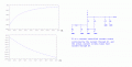
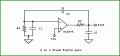
In the diagram shown in the attachment, i use a transistor model that is a current controlled current source with some low input resistance similar to the base emitter of the transistor. There will be a little feedback from the internal small re value, but that is ignored for now and this should not change the outcome by enough to invalidate the overall observation that the poles migrate in opposite directions as mentioned previously.
So now we use a model of the actual transistor circuit to evaluate the operation, and noteworthy is that there is a third capacitor added to the input, input to ground, and that may be necessary to see this effect. Without that input cap we might not see the pole splitting action, so i included it in the model circuit.
The values were C2=200pf, C3=20pf, R3=1, R1=300, R2=10, R4=100k. Note also that the current source "I" only changes the bias so it can be set equal to zero. Also note that R4=100k assuming the second transistor of the original circuit had a gain of around 100 and total emitter resistance of 1k. The gain of the first transistor is made equal to 100.
With all that in mind, the results are clearly showing the two poles moving in opposite directions, and that is graphed for values of C1 from 2pf to 20pf in the two graphs. The top graph shows one pole migration, and the bottom graph shows the other pole migration.
I still cant help but advise that you take a look at the op amp version of this and see how much simpler it is to figure out what is happening. I'll post the circuit if you would like to take a look.
We can analyze this if you like, and get the equation down to just one variable C3, vary that and see what it does to the poles. Note we have no current sources or biasing to muddy up the analysis.
I simply assume that the VAS gain is -500V/V. Therefore Cfb capacitor is virtually increased (|Av|+1) due to the Miller effect.
And this is why I multiply 2pF by 501 to get 1nF
Well, for upper pole and looking at the formula F2' = 0.16/(Rs||Rout||rpi * Cin2) the only change which has been there when Cfb is included is the inclusion of Rs and rpi....and the difference it makes is that it decreases the denominator and hence f2 increases which causes the pole to shift higher in frequency..right..
So why Rs and rpi gets included with the presence of Cfb..?? or how Cfb makes a difference by acting as a short...??
please clarify what is Rout ...is it the output resistance of the whole circuit..
and shouldn't it be Rout ≈ rpi||Rout1..rather than Rout ≈ rpi||Rout2..?? because second pole occurs due to Rout1...
 Facebook
 Google
 GitHub
 Linkedin
")