Facebook
 Google
 GitHub
 Linkedin
Hey guys. I have this homework where I have to simulate a circuit that implements an AND/NAND gate with Emitter Coupled Logic.
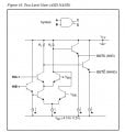
As I'm sure most of you know, the OR/NOR gates are the gates that are created the most with ECL technology. I searched online and found the model in the picture attached, which is supposed to implement a NAND/AND. How do I know which values I should put to the reference voltages (VBB1, VBB2)? Does anyone know if this circuit does indeed work to make a NAND/AND? Also, don't I need to add a current source between VEE and the emitters?
Thanks.
As I'm sure most of you know, the OR/NOR gates are the gates that are created the most with ECL technology. I searched online and found the model in the picture attached, which is supposed to implement a NAND/AND. How do I know which values I should put to the reference voltages (VBB1, VBB2)? Does anyone know if this circuit does indeed work to make a NAND/AND? Also, don't I need to add a current source between VEE and the emitters?
Thanks.
Attachments
-
 44.9 KB Views: 148