[Design] Two Stage Amplifier

Thread Starter

jegues

Joined Sep 13, 2010
733
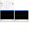
Alrighty here's another attempt at the simulation with some new values and my transistor orienated properly.

The input signal is on the LEFT and the output is on the RIGHT.

Is this what we would expect for such a circuit?:confused:
 

Attachments

If you want 50Ω output impedance, the second transistor emitter current Ie2 cannot be as low as 520uA.

This will set re2 to 50 ohms, but you also have to allow for Rc/(β+1) adding into the impedance.
The output resistance is Rc/(β+1) in series with re2 and that series combination in parallel with RE3. Ordinarily one might think that the parallel effect of RE3 would help bring down the output resistance so that a low emitter current could work, but RE3 can't be very low.

Since there is no load shown, apparently the second stage won't be expected to drive a 50 ohm load for this problem. It's a good thing, tool

If there were a load of 50 ohms with 6 volts P-P across it, that would be a dissipation of 90 mW in the load alone, exceeding the allowed 25 mW by a substantial margin.

However, if there is no load at the Vout terminal it's still possible for the output resistance to be < 50 ohms. The resistance at the collector of T1 is reflected to the emitter of T2 (a first cut calculation ignoring re2) as approximately Rc/(β+1), and this can be as low as 50 ohms if Rc is around 7500 ohms (if β=150); for an accurate value of the resistance at the emitter of T2 we need to account for re2, though. This can still give a swing of 3 volts if there is no additional load on the right end of Cc2, because RE3 need not be a low value to get 50 ohms at the emitter of T2; the low resistance can be provided by the reflected resistance.

If we assume a Vcc of 9 volts then 25 mW allows us a little more that 2.5 mA supply current. If Rc is around 7500 ohms, a quick calculation shows that for a first cut we can assume Ie1 of about .5 mA and Ie2 of about 2 mA. With Ie2 of 2 mA and 3 volts across RE3, then RE3 can't be any smaller than 1500 ohms.

If we let RE3 be 1500 ohms, and if we want the resistance at the emitter of T2 to be 50 ohms, then the reflected impedance from the collector of T1 to the emitter of T2 plus re2 must be 51.72 ohms (1500 ohms in parallel with 51.72 ohms is 50.00 ohms). If Ie2 is 2 mA, then re2 is 13 ohms and re2 is in series with the reflected impedance, and therefore Rc can't be any larger than (β+1)*(51.72-13) = 5847 ohms (for β=150).

Working our way in from the input side, if the resistance looking into the base is to be 25000 ohms (this would be the case if R1 and R2 are infinite, the limiting case; in reality this resistance will have to be larger to account for R1 and R2 being finite), then the quantity (β+1)*(re1+RE1) must be 25000 ohms, and (re1+RE1) must be 25000/(β+1) = 165.56. The gain of the first stage is Av = Rc/165.56; let's pick Av = 40 to make Rc as small as possible (to get as low a resistance reflected to the emitter of T2 as possible). Then Rc = 40*165.56 = 6622.51; Rc can't be any smaller than this.

We have a conflict. From the consideration of output resistance, Rc can't be any larger than 5847 ohms, and from input resistance considerations, Rc can't be any smaller than 6622 ohms. Apparently, a β of 150 isn't enough to complete the design. We can find a value of β which will make these two limiting values of Rc equal. I get about 160 for the result. It would probably be reasonable to require a β of 200 for this design to be practical.

Edit: You posted while I was working on my post. I see you have given RE3 the value I suggested. What β have you used in your simulation?

Are you assuming the requirement is for a 3 volt peak swing, or a 3 volt peak-to-peak swing? You can't get a 6 volt peak swing with only a 5 volt supply.
 
Last edited:

Audioguru

Joined Dec 20, 2007
11,248
Your output shows clipping because the transistors are not biased properly or the gain is too high or the input signal is too high.
 

Thread Starter

jegues

Joined Sep 13, 2010
733
The output resistance is Rc/(β+1) in series with re2 and that series combination in parallel with RE3. Ordinarily one might think that the parallel effect of RE3 would help bring down the output resistance so that a low emitter current could work, but RE3 can't be very low.

Since there is no load shown, apparently the second stage won't be expected to drive a 50 ohm load for this problem. It's a good thing, tool

If there were a load of 50 ohms with 6 volts P-P across it, that would be a dissipation of 90 mW in the load alone, exceeding the allowed 25 mW by a substantial margin.

However, if there is no load at the Vout terminal it's still possible for the output resistance to be < 50 ohms. The resistance at the collector of T1 is reflected to the emitter of T2 (a first cut calculation ignoring re2) as approximately Rc/(β+1), and this can be as low as 50 ohms if Rc is around 7500 ohms (if β=150); for an accurate value of the resistance at the emitter of T2 we need to account for re2, though. This can still give a swing of 3 volts if there is no additional load on the right end of Cc2, because RE3 need not be a low value to get 50 ohms at the emitter of T2; the low resistance can be provided by the reflected resistance.

If we assume a Vcc of 9 volts then 25 mW allows us a little more that 2.5 mA supply current. If Rc is around 7500 ohms, a quick calculation shows that for a first cut we can assume Ie1 of about .5 mA and Ie2 of about 2 mA. With Ie2 of 2 mA and 3 volts across RE3, then RE3 can't be any smaller than 1500 ohms.

If we let RE3 be 1500 ohms, and if we want the resistance at the emitter of T2 to be 50 ohms, then the reflected impedance from the collector of T1 to the emitter of T2 plus re2 must be 51.72 ohms (1500 ohms in parallel with 51.72 ohms is 50.00 ohms). If Ie2 is 2 mA, then re2 is 13 ohms and re2 is in series with the reflected impedance, and therefore Rc can't be any larger than (β+1)*(51.72-13) = 5847 ohms (for β=150).

Working our way in from the input side, if the resistance looking into the base is to be 25000 ohms (this would be the case if R1 and R2 are infinite, the limiting case; in reality this resistance will have to be larger to account for R1 and R2 being finite), then the quantity (β+1)*(re1+RE1) must be 25000 ohms, and (re1+RE1) must be 25000/(β+1) = 165.56. The gain of the first stage is Av = Rc/165.56; let's pick Av = 40 to make Rc as small as possible (to get as low a resistance reflected to the emitter of T2 as possible). Then Rc = 40*165.56 = 6622.51; Rc can't be any smaller than this.

We have a conflict. From the consideration of output resistance, Rc can't be any larger than 5847 ohms, and from input resistance considerations, Rc can't be any smaller than 6622 ohms. Apparently, a β of 150 isn't enough to complete the design. We can find a value of β which will make these two limiting values of Rc equal. I get about 160 for the result. It would probably be reasonable to require a β of 200 for this design to be practical.

Edit: You posted while I was working on my post. I see you have given RE3 the value I suggested. What β have you used in your simulation?

Are you assuming the requirement is for a 3 volt peak swing, or a 3 volt peak-to-peak swing? You can't get a 6 volt peak swing with only a 5 volt supply.
Thank you for the very detailed post The Electrician. We are told that the β values of our transistor is 150. However, we were also told that if need be we could loosen up the design criteria by about 10%.

Is this a big enough margin to fix any problems we might have without altering our β?

In any case, based on the previous simulation I posted, is there any resistance values should I alter? I took my Rc as 10k, should I lower that?

Are the values of RB1 and RB2 okay? Anything else I should tweak?

Thanks again!
 
You need to answer the last thing I asked you; it makes a big difference:

"Are you assuming the requirement is for a 3 volt peak swing, or a 3 volt peak-to-peak swing? You can't get a 6 volt peak swing with only a 5 volt supply."
 

Thread Starter

jegues

Joined Sep 13, 2010
733
You need to answer the last thing I asked you; it makes a big difference:

"Are you assuming the requirement is for a 3 volt peak swing, or a 3 volt peak-to-peak swing? You can't get a 6 volt peak swing with only a 5 volt supply."
Whoops, sorry, it should be a 3 volt peak swing.
 
It is crucial because 3 volts peak is the same as 6 volts peak-to-peak, and you can't get that with a 5 volt supply. If you only need 3 volts peak-to-peak (which is the same as 1.5 volts peak) then you can use a 5 volt supply.

If you can use a 5 volt supply then the 25 mW limit allows a total current of 5 mA rather than just 2.778 mA when you use a 9 volt supply.

It appears that with a 5 volt supply and a 3 volt peak-to-peak output swing requirement, the design is possible.

Revisit the calculations I described in the earlier post.

If you allocate ~.5 mA to T1 and ~4.5 mA to T2, then RE3 can be 330 ohms, and re2 is only 6.5 ohms. With RE3 equal to 330 ohms and Ie2 equal to 4.5 mA, the voltage across RE3 won't quite be 1.5 volts, but it's very close. You can later adjust Rc so that you get >1.5 volts across RE3, with slightly more than 4.5 mA in it.

Figure out what resistance needs to be reflected from Rc to the emitter of T2 so that the resistance at that emitter (reflected plus re2 in series with RE3 then in parallel) will be <50 ohms; this will give you a value for Rc, which should be larger than needed to meet the Av requirement.

R1 and R2 can be selected so that their combined parallel equivalent in parallel with the resistance looking into the base of T1 will be >25000 ohms.
 

Thread Starter

jegues

Joined Sep 13, 2010
733
It is crucial because 3 volts peak is the same as 6 volts peak-to-peak, and you can't get that with a 5 volt supply. If you only need 3 volts peak-to-peak (which is the same as 1.5 volts peak) then you can use a 5 volt supply.

If you can use a 5 volt supply then the 25 mW limit allows a total current of 5 mA rather than just 2.778 mA when you use a 9 volt supply.

It appears that with a 5 volt supply and a 3 volt peak-to-peak output swing requirement, the design is possible.

Revisit the calculations I described in the earlier post.

If you allocate ~.5 mA to T1 and ~4.5 mA to T2, then RE3 can be 330 ohms, and re2 is only 6.5 ohms. With RE3 equal to 330 ohms and Ie2 equal to 4.5 mA, the voltage across RE3 won't quite be 1.5 volts, but it's very close. You can later adjust Rc so that you get >1.5 volts across RE3, with slightly more than 4.5 mA in it.

Figure out what resistance needs to be reflected from Rc to the emitter of T2 so that the resistance at that emitter (reflected plus re2 in series with RE3 then in parallel) will be <50 ohms; this will give you a value for Rc, which should be larger than needed to meet the Av requirement.

R1 and R2 can be selected so that their combined parallel equivalent in parallel with the resistance looking into the base of T1 will be >25000 ohms.
Why would we want to use a 5v supply? In the design they require that you use Vcc = 9v.
 
Why would we want to use a 5v supply? In the design they require that you use Vcc = 9v.
Because as I said:"If you can use a 5 volt supply then the 25 mW limit allows a total current of 5 mA rather than just 2.778 mA when you use a 9 volt supply."

A larger current for Ie2 allows re2 and RE3 to be smaller which makes it possible to meet the output resistance requirement with a larger Rc.

Why did you use 5 volts in the simulation you posted in post #41 if you are required to use 9 volts? The image you posted in the first post doesn't say anything about 9 volts for Vcc.
 

Adjuster

Joined Dec 26, 2010
2,148
Note also that your input level is much too big, assuming that you have achieved the required gain of about 45 times. You have 120mVpk input. Times 45 gives 5.4V peak, or 10.8V peak to peak. That is too much even with a 9V supply.

Once you decide whether you want 3Vpk-pk or 3Vpk output, select the input voltage accordingly.
 

Adjuster

Joined Dec 26, 2010
2,148
A 9V solution will allow you about 2mA output stage bias current (re≈13.Ω) A transistor with Hfe>250 will then still allow you about 8K load and still meet the 50Ω output.

The 2N3904 and 2N3906 may not a terribly good choice for this circuit. The typical gains may be of the right order, but minimum values are lower. Of course, you may be limited by what's in your simulator, or available for a practical build.
 

Thread Starter

jegues

Joined Sep 13, 2010
733
Because as I said:"If you can use a 5 volt supply then the 25 mW limit allows a total current of 5 mA rather than just 2.778 mA when you use a 9 volt supply."

A larger current for Ie2 allows re2 and RE3 to be smaller which makes it possible to meet the output resistance requirement with a larger Rc.

Why did you use 5 volts in the simulation you posted in post #41 if you are required to use 9 volts? The image you posted in the first post doesn't say anything about 9 volts for Vcc.
That is my mistake. That Vcc should be 9V.
 
In post #32, Jony130 offered the opinion that with β=150 the design can't be done.

In post #42, I explained my reasons for believing that if Vcc=9V, β=150, and maximum power consumption is 25 mW, the design requirements can't be met.

You did say that the instructor will allow you to relax some things by 10%.

If you increase β by 10%, increase the target output resistance by 10%, decrease the target input resistance by 10% and decrease the minumum Av by 10%, I think you can complete the design with a 9V supply. In fact, you probably won't have to change all of those thing by 10%.

I would start by increasing β by 10%. If you still have trouble, next increase the target Rout by 10%.
 

Adjuster

Joined Dec 26, 2010
2,148
It cannot be done at all with β = 150. It's easy to see: Even neglecting re2, biggest Rc is 50Ω*(β+1) = 50Ω * 151 = 7550Ω.

For Av = 50, (Re1 + re1) = R7550/50= 151. Neglecting bias chain, Rin = 151*151 = 22.8kΩ.

With the bias chain included, the input impedance is lower still.
 
Last edited:

Thread Starter

jegues

Joined Sep 13, 2010
733
It cannot be done at all with β = 150. It's easy to see: Even neglecting re2, biggest Rc is 50Ω*(β+1) = 50Ω * 151 = 7550Ω.

For Av = 50, (Re1 + re1) = R7550/50= 151. Neglecting bias chain, Rin = 151*151 = 22.8kΩ.

With the bias chain included, the input impedance is lower still.
What would be the best possible design with what I've got to work with then? Is there one constraint I can sacrifice to salvage the others?
 

t_n_k

Joined Mar 6, 2009
5,455
What would be the best possible design with what I've got to work with then? Is there one constraint I can sacrifice to salvage the others?
I would simply make the perfectly justifiable case that if this is a design process with fixed design goals then as a designer, I would (at the very least) have the choice of transistor type. After all the teacher has said this is a self-driven learning exercise. If he/she gives you the task without any guidance, then you have control of the process and the right to make sound design choices including component selection. Transistors with β values >> 150 are readily available to the designer. The design goals are probably achievable with a β=200 and everything else the same.

The only concern I would have is that bias stability may be an issue - an important point which the teacher seems to have conveniently overlooked.
 

Adjuster

Joined Dec 26, 2010
2,148
You might want to think about how much of a constraint the base bias chain (RB1 and RB2) gives you. It is helpful to use large resistors here to avoid loading the input too much, but as the last post has perhaps alluded to, this conflicts with bias stability. Better bias stability is obtained by having the bias chain current a sizeable factor times the base current.

How many times Ib can you then have in the chain, without the impedance being too low? This depends in part on the base voltage: if the total chain resistance is R, then the lower resistor is R*Vb/Vcc, upper resistor is R*(1-Vb/Vcc). The parallel combination impedance is therefore R*(Vb/Vcc)(1-Vb/Vcc). This ignores the extra voltage drop due to the base current.

You should see that it helps to have the base voltage as close to half supply as possible, but probably about 2V on the emitter is a sensible upper limit if you want 6Vp-p output with a 9V supply. With Vb = 2.6V, base chain impedance, Zchain = R*0.288*(1-0.288) = R*0.205

For a 9V <25mW design, you might have about 2mA in T2, 0.5mA in T1, so T1 base current could be around 3.333uA with a gain of 150, or 2.5uA with a gain of 200.

Let's try a few values: chain current 10*Ib = 33uA , R = 9V/33.3uA = 270kΩ, Zchain = 55.5kΩ.
I chain = 5*Ib would give R=540kΩ, Zchain = 111kΩ.

If then we let the current gain reduce from 200 to 150, the base current increases by 0.833uA, so the base bias voltage drops by 46mV for 56kΩ impedance, or 92mV with 111kΩ. You might like to think whether that would be OK - the current gain may vary more than that. Note that your actual resistors need to be preferred values, set to get the voltage correct with the typical current gain.
 
Last edited:
Top