Current ratio, supply to power amp & across load

Thread Starter

PeteHL

Joined Dec 17, 2014
579
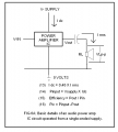
I'm posting Figure 6 and some formulas from an old magazine article about how to size a power supply to a selected power amplifier IC. I would like to understand the derivation of one of the formulas given in the article,

I-dc = 0.45 X I-rms

where I-dc and I-rms equal respectively current to the amp by the power supply and current in the speaker load connected to the amp. In the attached image, this is formula # 13. The author does not explain where the formula comes from.

In an example calculation of the article, the power supply voltage is made equal to the peak to peak voltage drop across the speaker load starting from a given wattage and known resistance of the load.

Thanks if you know,
Pete


MARSTON-FIG6.png
 

crutschow

Joined Mar 14, 2008
38,490
Since the current is drawn from the power supply only for the positive half-cycle, with the negative half-cycle current going to ground, the positive half-wave RMS current = 0.5 Irns.
By definition the RMS sinewave current is 0.707 Ipk and the average half-wave current is 0.637 Ipk.
From the above, the average Idc supply current is thus .637/.707 = 0.9 times the RMS, giving an average current of 0.9*.0.5 Irms = 0.45 Irms (QED).

Edit: This also shows the maximum efficiency of a Class B stage.
The load power is 0.707 Vpk x Irms and the supply power is 2Vpk x 0.45 Irms.
The efficiency is then 0.707 / 0.9 = 78.6%
 
Last edited:

Thread Starter

PeteHL

Joined Dec 17, 2014
579
Since the current is drawn from the power supply only for the positive half-cycle, with the negative half-cycle current going to ground, the positive half-wave RMS current = 0.5 Irns.
By definition the RMS sinewave current is 0.707 Ipk and the average half-wave current is 0.637 Ipk.
From the above, the average Idc supply current is thus .637/.707 = 0.9 times the RMS, giving an average current of 0.9*.0.5 Irms = 0.45 Irms (QED).

Edit: This also shows the maximum efficiency of a Class B stage.
The load power is 0.707 Vpk x Irms and the supply power is 2Vpk x 0.45 Irms.
The efficiency is then 0.707 / 0.9 = 78.6%
Thank you crutschow! I don't quite follow all of that, but I will give it some more thought. If the power supply were split (bipolar), would formula #13 still apply?
 

Thread Starter

PeteHL

Joined Dec 17, 2014
579
Since the current is drawn from the power supply only for the positive half-cycle, with the negative half-cycle current going to ground, the positive half-wave RMS current = 0.5 Irns.
By definition the RMS sinewave current is 0.707 Ipk and the average half-wave current is 0.637 Ipk.
From the above, the average Idc supply current is thus .637/.707 = 0.9 times the RMS, giving an average current of 0.9*.0.5 Irms = 0.45 Irms (QED).
1. If "current is drawn from the power supply only for the positive half-cycle", then from where does the amplifier draw current during the negative half-cycle? The ground connection is not a source of electrical power, only the power supply can provide that.

2. In the single-ended supply arrangement, the amplifier has a reference voltage equal to Vsupply divided by 2. This means that relative voltage applied to the amplifier is + or - one-half times the supply voltage. Thus it seems that in calculating input power from the voltage supply, Idc should be multiplied times Vsupply divided by 2. This is of course incorrect as then input power would then be less than output power. But I don't see the legitimacy of multiplying by the full supply voltage.

3. In the case of the split supply, Idc = 0.45 X Irms is "drawn from each supply", and assuming a split supply comparable to the single-ended one, the voltage of each supply is Vsupply (single-ended) divided by 2. Depending on polarity of the current through the load, then input power is equal to 0.5 X Vsupply X 0.45 X Irms.

Trying to search a different explanation for this on the web, the first result was this thread :(. I couldn't find a discussion of this in any of my books, either. So I hope that you don't mind this.
Regards,
Pete
 

crutschow

Joined Mar 14, 2008
38,490
1. If "current is drawn from the power supply only for the positive half-cycle", then from where does the amplifier draw current during the negative half-cycle?
It draws the current from the large output capacitor to the speaker, which is sitting at 1/2 the supply voltage.
It other words the capacitor is charged from the supply on the positive half-cycle, and is discharged to ground on the negative half-cycle.
2. In the single-ended supply arrangement, the amplifier has a reference voltage equal to Vsupply divided by 2. This means that relative voltage applied to the amplifier is + or - one-half times the supply voltage. Thus it seems that in calculating input power from the voltage supply, Idc should be multiplied times Vsupply divided by 2.
The power from the supply and to the amplifier is simply the supply voltage times the average supply current.
What the amp does with that voltage and current has on effect on the power drawn from the supply.
Relative voltage doesn't enter into the calculation as the power supply doesn't care what the amp does with the power.
 

Jony130

Joined Feb 17, 2009
5,596
It draws the current from the large output capacitor to the speaker, which is sitting at 1/2 the supply voltage.
It other words the capacitor is charged from the supply on the positive half-cycle, and is discharged to ground on the negative half-cycle.
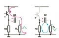
A picture is worth a thousand words.

0_1170101181.jpg
 

Thread Starter

PeteHL

Joined Dec 17, 2014
579
I do not understand your question. Can you elaborate more?
If you first charge a capacitor say with a DC voltage source, then switch to discharging the capacitor by a circuit of the capacitor and a resistor (such as the picture in your post #9), then the voltage drop across the resistor-load versus time is an exponential curve.

Maybe what Crutschow means is that by means of the output terminal of the amp connected to one of the terminals of the capacitor the amp controls the instantaneous rate of discharge of the output capacitor.

In a previous part of one of the series of articles that I referred to in my first post, I do see that the IC audio power amplifiers of the article when connected to a single-ended voltage supply are shown with a large (~2200 uF) capacitor connected to the output terminal of the amp.
 

crutschow

Joined Mar 14, 2008
38,490
The voltage versus time discharge curve of a capacitor hardly looks like a sine wave, let alone a complex music signal?
That depends on how you discharge the capacitor (I assume you are referring to the typical RC exponential capacitor discharge curve).
But, in this case, the capacitor is very large, so that it charges and discharges only a small fraction of its total charge for the music signal, so its change in voltage has no significant effect on the output waveform.

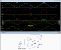
Below is the simulation of a simple emitter-follower complementary output stage to show this:
As expected, the NPN conducts for the positive half-cycle (purple trace) and the PNP for the negative half-cycle (orange trace), with the output load voltage and current going equally positive and negative (red and green traces).
Note the small change in voltage across the capacitor during each cycle (yellow trace). For such a small change, the RC charge and discharge curve is essentially linear and causes no detrimental effect (distortion) of the output waveform.

The slight glitch at the waveform zero crossings is the crossover distortion due to the transistor Vbe voltages (which is biased out in a practical amplifier).

Make more sense now?

upload_2019-2-4_13-54-39.png
 
Last edited:

Thread Starter

PeteHL

Joined Dec 17, 2014
579
That depends on how you discharge the capacitor (I assume you are referring to the typical RC exponential capacitor discharge curve).
But, in this case, the capacitor is very large, so that it charges and discharges only a small fraction of its total charge for the music signal, so its change in voltage has no significant effect on the output waveform.

Below is the simulation of a simple emitter-follower complementary output stage to show this:
As expected, the NPN conducts for the positive half-cycle (purple trace) and the PNP for the negative half-cycle (orange trace), with the output load voltage and current going equally positive and negative (red and green traces).
Note the small change in voltage across the capacitor during each cycle (yellow trace). For such a small change, the RC charge and discharge curve is essentially linear and causes no detrimental effect (distortion) of the output waveform.

The slight glitch at the waveform zero crossings is the crossover distortion due to the transistor Vbe voltages (which is biased out in a practical amplifier).

Make more sense now?

View attachment 169440
Thanks so much, that is an excellent explanation.

-Pete
 
Top