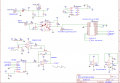
Does anyone know how the following capacitor and resistor values have been calculated? I am trying to learn how to pick values from a design perspective
Two important parameters in selection of resistors that are connected to the input of an op amp are the op amp's input bias/offset current and the circuit frequency response.
The resistors should be low enough that the stray capacitances don't degrade the highest frequency of interest, and the bias/offset currents don't cause an output DC offset that adversely affects the required measurement accuracy.
So once you the required frequency response and DC accuracy required for the circuit, you can then select appropriate resistor values.
But you can't use arbitrarily low resistor values to minimize the above effects.
The lower limit to the resistor values are determined by the required input impedance of the circuit to the signal source, and how much output current the op amp can provide to the output load and the feedback resistors.
So the balancing act is between wanting low resistor values to minimize the effects of stray capacitance and input bias currents, and wanting high resistance values needed to meet the input and feedback load impedance requirements.
So you try to pick some intermediate values that satisfy all the requirements.
In some cases this gives you a narrow selection (or no selection).
In other cases there can be a large selection of values to meet all the requirements. In that case you can select some arbitrary values somewhere in between.
C8 and R7 are chosen based on the frequency of the incoming square wave. R1 and R5 were probably chosen to consume little current from the 5V supply. The TL084 has JFET inputs so large resistors don’t pose much problem. I can’t say anything about R6 without seeing where it goes.
I have attached the full schematic to show where the output resistor goes. The frequency of the incoming square wave is between 30Hz and 1000Hz.
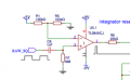
I understand that the RC form a High Pass filter, only allowing higher frequencies, thus creating a spike effect. However according to calculation, the cut off frequency is around 23kHz. which is much higher than the frequency range from the PWM. Will this not completely stop all frequencies?
And if the HPF is already generating a spike effect, why is a comparator needed? thanks
The junction of C8 and R7 has transients in both directions around the middle point of the signal, at both the positive-going and negative-going transitions of the incoming square wave. The comparator allows the output to go high only on the positive-going transitions. Otherwise the output sits at the negative saturation voltage, which turns off J1 fully since the source is at virtual ground. Also it provides drive current for the transistor gate.
I understand that the RC form a High Pass filter, only allowing higher frequencies, thus creating a spike effect. However according to calculation, the cut off frequency is around 23kHz. which is much higher than the frequency range from the PWM. Will this not completely stop all frequencies?
No, it won't; the PWM signal contains not only it's base frequency, but many harmonics of the base frequency.
But rather than think in terms of frequency, and filtering, think instead of R7 and C8 as a differentiator circuit with an RC time constant of 6.8 kΩ * 1 nF = 6.8 μs: on the rising edge of the PWM signal, it lets through a short positive pulse to pin 3 of U5.1 (actually, a waveform with a sharp positive leading edge, followed by an exponential decay back down to zero); and on the falling edge of the PWM signal, it lets through a short negative pulse. Because of the way the inputs of U5.1 are biased, only the positive pulse has any effect; the op amp, which is used as a comparator in that part of the circuit, "squares up" that pulse to produce on its output an approximately rectangular pulse of roughly 5 μs duration to drive the gate of JFET J1.
Thank you, that makes sense. So i suppose the design approach was to design a RC differentiator that created a pulse of approx 5us? then choosing components that closely matched that spec?
The clock in the micrcontroller was prescaled, giving a time period of 5us (Making each tick duration 5us) Would this be related to reason for the pulse length ?
Thank you, that makes sense. So i suppose the design approach was to design a RC differentiator that created a pulse of approx 5us? then choosing components that closely matched that spec?
Yes, although that "spec" may have only been approximate, like "need a pulse long enough to ensure the integrator gets reset."
The clock in the micrcontroller was prescaled, giving a time period of 5us (Making each tick duration 5us) Would this be related to reason for the pulse length ?
I rather doubt it, as the pulse seems to be used only to turn on J1, resetting the integrator. It doesn't appear to go to the microcontroller or anywhere else.
But surely the length of the pulse is defined by the the length of the time it takes for the integrator to reach 0v? Would a longer pulse not hold the integrator at 0V, and a shorter prevent it from reaching 0v? Or am I not understanding it properly?
But surely the length of the pulse is defined by the the length of the time it takes for the integrator to reach 0v? Would a longer pulse not hold the integrator at 0V, and a shorter prevent it from reaching 0v? Or am I not understanding it properly?
Some things in electronics need to be exact or precise. Other things need only be approximate. I imagine the requirement here was something like "long enough to ensure the integrator capacitor is completely discharged, but not ridiculous."
Actually, since this is a pulse forming circuit, C8 and R7 are chosen to define the width of the output pulse required to reset the integrator, based on the R1-R5 trip point. The timer is triggered by the input waveform positive edge, so the output pulse must be more narrow than the input waveform's minimum positive half-cycle pulse width. As long as the output pulse is less than 20% of the input waveform's negative half-cycle pulse width, C8 will have enough time to recover before the next positive edge. Thus, C8-R7 are related to different parameters of the input's two half-cycles, not simply its frequency.
Also, the reset pulse calculates out to less than 5 us. Are you sure the opamp can produce such a narrow pulse cleanly?
the output pulse must be more narrow than the input waveform's minimum positive half-cycle pulse width:
by input waveform, do you mean the waveform that is outputted from the DAC to drive the sawtooth? In that case, the minimum time period of the signal at the highest note is 239 us. which is 119.5 us for half-cycle.
I am a bit confused when you mention the negative half cycle, surely it will be equal to the positive? if this is the case, 20% of 119.5 us is 23.9 us. where did you get the 20% value from ?
Did you calculate the the reset pulse using the time constant equation as OBW0549 showed above?
the output pulse must be more narrow than the input waveform's minimum positive half-cycle pulse width:
by input waveform, do you mean the waveform that is outputted from the DAC to drive the sawtooth?
During the positive half-cycles, C8 is charged through R7; during the negative half cycles, it is discharged through R7. For consistent pulse widths, you want C8 completely discharged before the next positive edge comes along. Standard engineering time constant approximations:
1 TC = 63%
2 TC = 86%
3 TC = 95%
4 TC = 98%
5 TC = 99%
If the negative half cycle is 5 times as long as the intended output pulse width, the cap will be 99% discharged before the next event. ***Hmmm - the actual discharge conditions are a bit more complex than that (reaching 99% discharged will take 6 or 7 TC, not 5), but it still is a good approximation for this application.
Did you calculate the the reset pulse using the time constant equation as OBW0549 showed above?
Ah ok, so we are waiting 5 x the minimum half cycle value in order to allow the capacitor to discharge properly. So since it is a 50/50 duty cycle and the a minimum half cycle is 119.5 us. we need a pulse that is less than 24us to avoid any issues at the RC differentiatior.
Is the constant 4.71us pulse not control the duration that the integrator (C9) discharges at all?
Am i right in thinking that the 4.71us pulse is also the time given for C9 to dishcarge too (thus creating the discharge of the sawtooth)? therefore shouldn't its value be taken onto consideration here too? Or will be the sawtooth reset regradless of how long the pulse is?
Sorry to have to step through this, but it is easy get confusing.
The cap I'm talking about discharging is the timer cap C8, not the integrator cap. 4.7 us is the width of the pulse at U5 pin1. How that affects the integrator, is it too narrow to properly reset the integrator cap, is it unnecessarily wide - don't know.
Hi, I just wanted to bring up this post again. I am trying to design a new DCO circuit. I am wondering if anyone knows how to calculate the time taken for the integrator's feedback capacitor C9 to discharge? Looking at the simulation, the sawtooth ramp reaches 4.5V, and it discharges to 0V at time of around 3.4us. is there a way to find this time through calculation? Im not sure if the resistor R8 is considered to be in series during this time ? Also, I would have thought that the FET will have some forward voltage, thus prevents the capacitor from sully discharging ?
In your application the FET is acting as a voltage-controlled resistor. As such, it does not have a minimum voltage drop across it (unlike a bipolar transistor) - as long as the voltage relationship between the gate and source is correct.
 Facebook
 Google
 GitHub
 Linkedin
 25.9 KB Views: 61