Facebook
 Google
 GitHub
 Linkedin
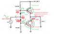
Hello
Hope you are all good,
Can someone explain how does the compensating diodes work during the positive and negative half cycles input signals of push pull amplifier?
Thanks and regards
SM
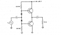
Hope you are all good,
Can someone explain how does the compensating diodes work during the positive and negative half cycles input signals of push pull amplifier?
Thanks and regards
SM
Attachments
-
 11.7 KB Views: 186