That gives us nothing to go on. We will not do your homework for you. You need to show YOUR best attempt to solve the problem. We can then look it over and point out where you are making a mistake or give a hint on what you might need to consider. But YOU need to do the work.
That gives us nothing to go on. We will not do your homework for you. You need to show YOUR best attempt to solve the problem. We can then look it over and point out where you are making a mistake or give a hint on what you might need to consider. But YOU need to do the work.
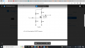
There are a few different symbols that are used and a lot of people are sloppy about using the correct symbol.
But the symbol in your problem statement is usually the one for a depletion mode device. Notice that there is a continuous path between drain to source -- this is indicative of the behavior that, without any gate voltage applied, the device is conducting.
The symbol for an enhancement mode device generally looks something like:
The breaks between drain and source indicate that it is non-conducting when no gate voltage is applied.
If you know that the current into and out of the gate is zero, or so close to zero as to not be worth worrying about, then all of the DC currents in the gate circuit must flow through the resistors, does that help? It should because Ohm's law will tell you the current through the resistors, whose values are known, if you know the voltage across them.
Here is what Infineon says about depletion mode MOSFETs:
The features of a single current regulator in one component Infineon is one of the few semiconductor manufacturers worldwide to offer N-channel depletion mode MOSFETs. Compared to enhancement mode transistors, known as normally-off, depletion MOSFETs are in an on-state at zero voltage of gate-to-source (VGS), normally-on. This makes N-channel depletion MOSFETs a perfect constant current source.
(Emphasis added) Source: https://www.infineon.com/cms/en/product/power/mosfet/n-channel-depletion-mode/
The above is consistent with what @WBahn said post #10: But the symbol in your problem statement is usually the one for a depletion mode device. Notice that there is a continuous path between drain to source -- this is indicative of the behavior that, without any gate voltage applied, the device is conducting.
So look in your textbook, or wherever, for the equations that govern the behavior (the voltage/current relationship) for a depletion mode MOSFET. Stop just expecting others to spoon feed you the basic information you are supposed to be learning.
Actually, there is enough info given to calculate the answers for any black box if you assume the gate is insulated from the drain. You do not need to know anything about the device.
Actually, there is enough info given to calculate the answers for any black box if you assume the gate is insulated from the drain. You do not need to know anything about the device.
So you are saying that the answer is exactly the same whether the FET is enhancement mode or depletion mode, or whether the device is N-channel or P-channel? Or if the device is a VCCS or a VCVS?
Since we don't need to know anything about the device if we assume that the gate is insulated from the drain, we can assume that the device is an open circuit. Thus there is no drain current flowing at all.
Since we don't need to know anything about the device if we assume that the gate is insulated from the drain, we can assume that the device consists of a short between drain in source, Thus the drain current is 19.35 mA.
Seems like we might need to know a little bit more about what's in that box beyond the gate being insulated from the drain.
 Facebook
 Google
 GitHub
 Linkedin
 140.7 KB Views: 26


")


