Arduino Driving a relay_Schematic Review /suggestions

Thread Starter

hoyyoth

Joined Mar 21, 2020
309
Dear Team,

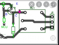
I using Arduino nano to drive this relay.P/N is G5NB-1A-E DC5. My circuit is given below.

May I know this circuit is fine or not?

V_CHIP_REL1_EN is coming from Arduino Nano

My diode P/N is S1MTR

May I know things that needs to be considered for PCB layout.
  1. According to me Relay needs a solid return path.
  2. No trace routing below the realy.
Is this fine.

1636187685337.png

Regards
HARI
 
Last edited:

Thread Starter

hoyyoth

Joined Mar 21, 2020
309
Hi Eric

Please see my answer below.

What else is on the PCB,?

Couple of CMOS Switches(,SPDT,SPST),One Unity gain buffer,I2C level translator.

What is the project designed to do.?

ASIC characterization board.

Regards
HARI
 

ericgibbs

Joined Jan 29, 2010
18,849
Hi Hari,
Seems to be a simple PCB layout.
Which Artwork program are you using.?

I would suggest you create a draft layout diagram, so that we can check.

E
 

Thread Starter

hoyyoth

Joined Mar 21, 2020
309
Al
Hi Hari,
Seems to be a simple PCB layout.
Which Artwork program are you using.?

I would suggest you create a draft layout diagram, so that we can check.

E
Allegro
Layout will not be that complicated.

My only concern is if traces are routed below the really, will magnetic energy from relay coil will couple to the trace.
 

ericgibbs

Joined Jan 29, 2010
18,849
hi Hari,
For such a simple circuit, the track path is not critical.
ie: No RF, No very low analogue signals etc.

Place the relay, so that the edge of the PCB has a two-way terminal block for the relay output contacts.

Have you decided what shape/profile the overall PCB has to be,
eg: does it have to fit in a certain place on the project or say in an enclosure.??

E
Added. Example.
Note, ensure that your relay footprint/pads match your relay..
 

Attachments

Last edited:

ericgibbs

Joined Jan 29, 2010
18,849
hi,
What will be connected to the relay output terminal block.?
E


Update:
Add this PDF to your database files.

Clip from Page #9.
An old saying is that PCB design is 90% placement and 10% routing. Whilst the actual figures are of no importance, the concept that component placement is by far the most important aspect of laying out a board certainly holds true.
Good component placement will make your layout job easier and give the best electrical performance. Bad component placement can turn your routing job into a nightmare and give poor electrical performance.
It may even make your board unmanufacturable. So there is a lot to think about when placing components!
Every designer will have their own method of placing components, and if you gave the same circuit (no matter how simple) to 100 different experienced designers you’d get a 100 different PCB layouts every time.
So there is no absolute right way to place your components. But there are quite a few basic rules which will help ease your routing, give you the best electrical performance, and simplify large and complex designs.
At this point it is a good idea to give you an idea of the basic steps required to go about laying out a complete board:

Ø Set your snap grid, visible grid, and default track/pad sizes.
Ø Throw down all the components onto the board.
Ø Divide and place your components into functional “building blocks” where possible.
Ø Identify layout critical tracks on your circuit and route them first.
Ø Place and route each building block separately, off the board.
Ø Move completed building blocks into position on your main board.
Ø Route the remaining signal and power connections between blocks.
Ø Do a general “tidy up” of the board.
Ø Do a Design Rule Check.
Ø Get someone to check it
This is by no means a be-all and end-all check list, it’s highly variable depending on many factors. But it is a good general guide to producing a professional first-class layout.
Lets look in more detail at the procedure described above.
 

Attachments

Last edited:
Top