Adjustment of Dead Time between two gate signals

Thread Starter

scene

Joined Sep 9, 2010
7
Hi Everyone,

I am in need of assistance to come up with a circuit that enables me to control the dead time switching between two pwm signals.

The circuit operating characteristic is like this.

PWM Signal -> Adjustable Dead Time Circuit -> Producing two gate driving signals -> Driving a Voltage Source Inverter.

Apparently the current dead time circuit i have, is not able to adjust the signal between the two gate driving signals. The dead time between both of this signals are 120us, which is not ideal as short circuit might occur when both signal reaches '1' at the same period. Therefore i need a dead time which is 1.5 to 2us to allow my VSI to have a stable switching process.

Anyone can assist me, thanks.

Regards
JP
 

Dyslexicbloke

Joined Sep 4, 2010
566
You will need to post your circuit for that to make much sense.
It would also help if you could draw / sketch the output you require and indicate from what edges your times need to be initiated.

I dought the solution will be too complex once all the requirements are defined accuratly
Al
 
Last edited:

eblc1388

Joined Nov 28, 2008
1,542
The dead time between both of this signals are 120us, which is not ideal as short circuit might occur when both signal reaches '1' at the same period. Therefore i need a dead time which is 1.5 to 2us to allow my VSI to have a stable switching process.
Your post is not making sense.

Do you need dead time of 1.5~2ms?
 

Thread Starter

scene

Joined Sep 9, 2010
7
Hi there people, i have attached this file, and stated the problem... Please kindly assist.

I think is 1.5us to 2us, as what my colleague wants me to do.

Regards
Jingpo
 

Dyslexicbloke

Joined Sep 4, 2010
566
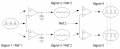
Please confirm that what you have now, I have correctly interpreted in terms of its 'intended' functionality.
[See attached]

The first two amps compare Sig1 with Ref1, indipendantly, and generate sawtooth waves that you intend to have the same magnitude freequency and offset but be inverted with respect to each other.

The second two amps share a common Ref2 and produce indipendant but complimentary, the same but inverted, square wave outputs who,s edges ar in phase.

If I am correct thus far you already have some issues and I am unsure what you are trying to achieve with the output ... what are you driving?

If I have it wrong please explain how it should function in terms of Sig# and Ref#
Al
 

Attachments

Last edited:

Thread Starter

scene

Joined Sep 9, 2010
7
Yes, you are correct. My problem now is to try control the dead time between both switching. From your posted figure, there is a missing potentiometer at the Ref 2. My original post indicates where the problem lies. I am to adjust the dead time between the two signals, approximately 1.5us to 2us. I will be using this signal to drive the SKM 50 GB 123 D, an IGBT circuit.
 

SgtWookie

Joined Jul 17, 2007
22,230
You need to split Ref2 into Ref2A and Ref2b; the difference in their voltage vs the rise/fall times will determine the difference in turn-on/turn-off times.

Unfortunately, capacitors have relatively high tolerance, and you are using separate caps in the outputs of your first pair of comparators/opamps (whichever) so you will likely have quite a difference in your output signals.

If you are going to continue with your current scheme, you will have to use matched comparators or opamps and matched capacitors. This will not be trivial, and it will be expensive to implement on any kind of large scale.
 
Absolutly agree with SgtWookie ...

I was planning on suggesting a diferent arrangement with a single base oscillator which is why I didnt show any ajustment.
Do you want to go that way?
Al
 

Thread Starter

scene

Joined Sep 9, 2010
7
Firstly, i want to thank you all for the support and suggestion you have given me. It really helps. By the way i repost this problem again in file "Reviewing Problem ", with the picture of the PWMTemp that Dyslexicbloke has posted to assure that we are actually looking into the same problem.

Main Focus

I am actually designing a Shunt active filter to compensate the harmonics that occurs when non linear loads are being used. This filter will act as a compensator at the point of common contact (PCC), where harmonics begins to occur from the existence of non linear load that is being used frequently in current commercial/industrial environment settings.

To: SgtWookie

Hi Sgtwookie, i am not working on big circuitries, but is it a must to separate the signals, cause from my fellow phd student. He emphasize that the two signal at ref 2 must know each other, therefore they can produce the correct signal at the output as what he stated.

Is it ok if i use capacitor that has lower tolerance, or smaller capacitor value that is significant enough to stablise the signal at the ref 2? I am also not working on a bigger circuits, therefore will it be ok?

To: Dyslexicbloke

Hi Dyslexicbloke, Will it help, i will like to try that. Do you have the circuit? Is it capable of controling the dead time of the circuit?

Review of problem in waveform
Anyways guys, i have uploaded some results on to this post in file "Waveform" & "Waveform End Result". The purpose of the potentiometer is to allow me to adjust the dead time, but unseemingly the yellow signal keeps shifting to a dead time end result of 120us. I can't decipher the problem, as my circuit analysis skills are limited, is it because the potentiometer is not met to adjust such signal. Or is it because the capacitor 470pf is charging and discharging the signal? Any solution?


Regards
scene
 

Attachments

Yes it will definatly help, if you are trying to produce complimentary signals then a comon source is effectivly a given. The reference to splitting the ref is to create a window during which neither output is on.

By the way ... I there a 'propper' way to draw a functional diagram that would convey the info I posted.
Anyone know?

Back with a mod for you shortly.
'O' and I am going to say now there are many folk on this board far better qualified/able to design the electronic solution, give it values and make it functional rather than conceptual.
I plan to give it a try so I can learn from the experiance .... just wanted to let you know exactly where we are both at.
Al
 

SgtWookie

Joined Jul 17, 2007
22,230
OK, then here's an alternative that will likely prove much easier to implement.

Rather than attempt to take an input square wave and convert it to two complementary triangle waves in one step, take the input square wave and convert it to a triangle wave.

Then to avoid problems with propagation delays, etc - run the signal through both an inverting and an non-inverting opamp. Make the non-inverting opamp's feedback path adjustable; in that manner you can control the dead time.

If you are in a Doctorate program and can't figure out how to post a .png image, then you need to figure out how to do that by yourself. MS Word .doc formats are very large, and take too much time for me to download. If you want me to look at your stuff, you better post it in .png format.
 
Hi, sorry I didnt post yesterday, I was sick and in bed for 24Hrs.
SgtWookie has your back here and is far better at this stuff than I am.

I would be happy to continue to help but probably not your best choice because although I could give you a solution it is unlikly that it would be ideal or even properly expressed.

My strap line is the most accurate thing I ever say ... take note!

I will keep monitoring the thread so I can learn too, just shout if you want anything.

Al
 
Top