A strange H bridge circuit, How does the Nmosfet drived?

Thread Starter

vincentcheng

Joined Jul 10, 2024
4
H.PNG
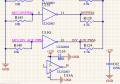
Hi, everyone. I have a schametic that quite confusing me. as far as I know, one should apply the Vgs voltage about 12V to drive the NMOSFET,
but here it seems no a GND for reference. drv.PNG
the BUS- is the battering minus and it is the primary side "gnd" in a flyback converter to make 12V, where the GND is pull out from secondary, there is no electrical connection for them both.

In this case, How can the MosFET be drive? it seems the S terminal is floating?
 

Thread Starter

vincentcheng

Joined Jul 10, 2024
4
There is not enough diagram shown to sort this out, where does INVPWM+G come from?
Hi, Sensacell , thank you for your answer. here is more information about the driving signal.
it seems they should be connected externally by a wire. some times to connect a test equipment in series? wire.PNGwire2.PNGdrvie.PNG
 

Attachments

Orson_Cart

Joined Jan 1, 2020
110
you need to research: " bootstrapped gate drive power supply " and chips like the IR2113 for high and low side driving of gates - the iC has an internal level shift. The data sheet for these GD IC's does a pretty good job of explaining all.
 

MisterBill2

Joined Jan 23, 2018
27,174
Since no connection to the mosfet source side is shown, the truth is that the circuit shown will not function because there is no mosfet gate drive. . So what you see is not a working design as it is presented.

Much like a story with words left out.
If the connections not shown are added then the circuit might work.
So your question is indeed proper, because AS SHOWN the circuit does not work. Wishing it would work does not help.
 
Top