Facebook
 Google
 GitHub
 Linkedin
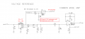
Attached is the input stage schematic of the Analog Devices pulsar A/D module.
For the ADC driver they used ADA4841 op-amp that has maximum 12V Vcc - Vee voltage, so op amps are powered with +7.5V and -2.5V
As the module is designed in sample differential signal in the -5V to 5V range they added summing point on each op-amp input raising each input by 2.5V through the simple voltage divider + filtering stage with 10u and .1u caps
Vcm is 5V and comes from 5V reference
My question is, why do they make things complicated? Since they powered op-ams with Vee of -2.5V they had to add 5V reference, filtering stage and precise matched resistors R1 R2 R3 and R4
in addition, using 590ohm on the input resistors will only work for low impedance sources and sources that can provide almost 10mA of current
Why not to choose op-amp that can be powered to Vee <-5V, then none of the above would be necessary.
Am I missing something here?
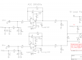
Attachments
-
 50.9 KB Views: 7