I changed it to 100Ω to get better filtering, as an increase in the resistor value has no significant effect on Vdd since the current draw is very low.On first layout you have resistor R3 10? and second layout R3 100
ok thanks ,, i draw on sheet on previous conversation layout pin numbers on cd4093 just could you confirmed if that is correct?I changed it to 100Ω to get better filtering, as an increase in the resistor value has no significant effect on Vdd since the current draw is very low.
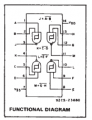
Ok i want to ask usually in front of transistor is resistor to prevent damage in your circuit is not is that okThe pin diagram from the data sheet is below so yes, your diagram looks correct.
(Be sure and tie the other unused inputs (not outputs) to ground.)
View attachment 169709
Yes.Ok i want to ask usually in front of transistor is resistor to prevent damage in your circuit is not is that ok
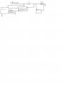
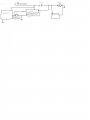
beeping more likely after 30km speed and ist annoing, i need then turn off with out pressing the switch,perfect solution would be activate and deactivate by speed but that is cam buss signal i can not brake,,,i draw small circuit how i think it could operate but i need to design timer for this, again thanks if you got a time to look at it