5-Bit SAR-ADC

Thread Starter

Fredi

Joined Jan 28, 2021
11
Hello everyone,

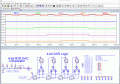
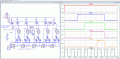
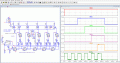
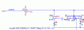
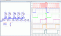
Currently, I'm doing my masters degree and working on a 5-Bit SAR-ADC design in LTSpice. The problem is the output signal is the same no whether what input signals I've got. As an example Vin is 5V and Vref is 2V. There could be problems with SAR Logic at the end of the circuit or the clocks are false. But actually I don't have any idea what to do to solve the problem.

Hopefully one of you can help me.
Kind regards Frederik
 

Attachments

Thread Starter

Fredi

Joined Jan 28, 2021
11
hi Fredi,
Welcome to AAC.
This is a working 4 bit SAR, I used sometime ago may give you some pointers.
E
Thank you ericgibbs for your quick answer. Your SPICE-Files are helping me a lot. Just another question: Do you know at which point in the logic we get the actual result ? Is it b0-b3 ? Because it's always the same signal. And what is your reference voltage (Vref) in Volt?
 

Thread Starter

Fredi

Joined Jan 28, 2021
11
hi F,
This LTS asc has been annotated.
Read the result on the falling edge of Clock pulse #5
E
Hi E,
In the SPICE-File you've got a SAR table. And I'm not sure if got it right.
As an example Ain=1,2 V and the result of the conversion should be b3=1, b2=1, b1=1, b0=1 at the falling edge of the fifth clock cycle?
F
 

ericgibbs

Joined Jan 29, 2010
18,766
hi,
Yes, thats how the original author of the file explained the operation.
Are you having a problem with the asc file.?
E
 

Thread Starter

Fredi

Joined Jan 28, 2021
11
hi,
Yes, thats how the original author of the file explained the operation.
Are you having a problem with the asc file.?
E
Hi,
No I don't have a problem with .asc file. When I'm plotting all bits in different panes and watch for the fifth falling edge of the clock. I can read the result of the conversion in the signal curve of b0-b3 there. Because I'm not getting the right results as shown in the table. Other question would be: What is the value of the reference voltage in the first cycle?
F
 

ericgibbs

Joined Jan 29, 2010
18,766
hi,
One point I was planning to change was the VCC of the digital IC's from1.0V to say 3.3V.
Using only 1.0v, limits the resolution of the comparator OPA.

Change the the VCC to to 3.3V and post your asc file, I will check you sim out for accuracy.
E
 

Thread Starter

Fredi

Joined Jan 28, 2021
11
hi,
One point I was planning to change was the VCC of the digital IC's from1.0V to say 3.3V.
Using only 1.0v, limits the resolution of the comparator OPA.

Change the the VCC to to 3.3V and post your asc file, I will check you sim out for accuracy.
E
Hi,
I've tried a few things to solve my problembut it still doesn't work. Maybe if you got a bit of time you may have a look on my schematic. I used your SAR Logic and added one more stage to get a logic for the 5 Bit. But with my capacitor array it doesn't work anymore.
F
 

Attachments

ericgibbs

Joined Jan 29, 2010
18,766
hi F,
I have cleaned up the circuit layout, it was messy and prone to reading errors.
Check the S10 and S5 Switches for correct connection.??

Also check the 'weighting' order of of C7 thru C12 caps.

In order to test the SAR I have temporarily connected the count input to Ub1 +5v

E

BTW: As this is a Homework assignment I am only giving guidance, not a final solution.
 

Attachments

Thread Starter

Fredi

Joined Jan 28, 2021
11
Hi Eric,
Thank you very much that's awesome you helped me a lot. I don't know how I'm gonna thank you for that. You spended a lot of time. I'm gonna try the rest on my own.
Have a good day,
Fredi
 

ericgibbs

Joined Jan 29, 2010
18,766
hi Fredi,
One last point I would note, is that you use the high impedance input [ NIV] of the OPA for the Capacitor array.
E
 

Thread Starter

Fredi

Joined Jan 28, 2021
11
hi eric,
It's been a while since the last time we talked. In the meanwhile I've done a lot of new versions of the SAR ADC. I'm still got problems to get the right results. You will notice that a lot of new stuff is going on there. Maybe you find time to have a look.
Kind regards,
F
 

Attachments

Thread Starter

Fredi

Joined Jan 28, 2021
11
hi eric,
When I'm feeding the circuits with different Vin and Vrefs there must be right reults.
As an example: Vin=0,4V Vref=1V. The result must be 00110. But that's not the case.
I'm getting the result 11111.
Fredi
 

ericgibbs

Joined Jan 29, 2010
18,766
hi F,
On that LTS asc, you appear to have two different circuits.
BTW: I did mention in a previous post, you have the sample/hold capacitors connected to the INV input of that OPA comparator.

What are the specifications or type code for that U1 OPA/Comp.?

Personally I prefer the resistive ladder network for determining of the 'weighting' of the Q0 thru Q4 outputs.
Is your assignment to design a capacitive sample/hold network.?

E


AAA 1206 12.26.gif
There is a drawing error here.
 

Attachments

Last edited:

Thread Starter

Fredi

Joined Jan 28, 2021
11
hi E,

The upper circuit is just a circuit to safe the values from the conversion.
The circuit below is the actual SAR ADC.

You mean that I have to plug the capacitor array to the positive input of the opamp?

The specs of the opamp are in the picture below.

Yes the assignment is to design a capacitive SAR network.

F
 

Attachments

ericgibbs

Joined Jan 29, 2010
18,766
hi F,
This is circuit section of the Counters/Gates, I have set Cout at +5V in order to Enable the circuit.
As you can see the Counter/Gates are generating the correct Binary Cout sequence

I will look at the Switch Array and check that for the correct function.[ it is a bit 'messy'] :rolleyes:

Is there any reason that you have chosen a +/-5V supply and Logic.?

Did you fix that open circuit in post #18.?

E
 

Attachments

Top