 Facebook
 Google
 GitHub
 Linkedin
This coursework involves the design and simulation of a synchronous sequential counter using a traditional approach employing small scale logic components and a modern approach using behavioural modelling with VHDL. The design specification for each student is unique and based on their student ID number.
The digits in your ID number, in the left to right order are used to specify the sequential output that a synchronous counter will produce in response to applied clock pulses. Assume that the ID digits are represented in a conventional 4-bit BCD code. The behaviour required of the counter is that it produces a 4-bit digital output that represents the BCD value of the successive digits of your ID number in the left to right sequence above. Once the right hand digit is output the counter will go back to the first and the sequence repeats. Note the digits represent the outputs of the counter and not its state variables. If your ID number is even you must implement the counter with JK flip-flops, if it is odd you should use D-type flip-flops.
-------->>>>>>>>>ID NUMBER = 4157241
1. Traditional design
Draw a state diagram to represent the behaviour of the counter you are required to design. It is suggested you employ the letters of the alphabet to refer to each state and keep the outputs as decimal numbers at this stage.
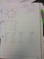
Insert state diagram here. (2 marks)
Convert the state diagram into its associated state table.
Insert state table here. (2 marks)
Assume that a simple binary state variable allocation can be made and that any unused states can be treated as don’t cares. Draw the corresponding transition table for the counter including flip-flop inputs and BCD outputs for your designated storage device.
Insert transition table here. (4 marks)
Using excitation maps determine the next state logic functions that can be used to drive your flip-flop inputs.
Insert excitation maps clearly showing groups and logic functions here. (6 marks)
Also draw Karnaugh maps to deduce minimal logic functions for the 4 output functions that are required to give the BCD output codes. Note that depending on your ID number not all outputs will be significant in all cases.
Insert the output function maps and logic equations here. (5 marks)
Enter the associated schematic circuit diagram here. (6 marks)
Hey guys I m Stuck with the Excitation map and K-map reduction. Could somebody explain how to solve it?
Thanks
The digits in your ID number, in the left to right order are used to specify the sequential output that a synchronous counter will produce in response to applied clock pulses. Assume that the ID digits are represented in a conventional 4-bit BCD code. The behaviour required of the counter is that it produces a 4-bit digital output that represents the BCD value of the successive digits of your ID number in the left to right sequence above. Once the right hand digit is output the counter will go back to the first and the sequence repeats. Note the digits represent the outputs of the counter and not its state variables. If your ID number is even you must implement the counter with JK flip-flops, if it is odd you should use D-type flip-flops.
-------->>>>>>>>>ID NUMBER = 4157241
1. Traditional design
Draw a state diagram to represent the behaviour of the counter you are required to design. It is suggested you employ the letters of the alphabet to refer to each state and keep the outputs as decimal numbers at this stage.
Insert state diagram here. (2 marks)
Convert the state diagram into its associated state table.
Insert state table here. (2 marks)
Assume that a simple binary state variable allocation can be made and that any unused states can be treated as don’t cares. Draw the corresponding transition table for the counter including flip-flop inputs and BCD outputs for your designated storage device.
Insert transition table here. (4 marks)
Using excitation maps determine the next state logic functions that can be used to drive your flip-flop inputs.
Insert excitation maps clearly showing groups and logic functions here. (6 marks)
Also draw Karnaugh maps to deduce minimal logic functions for the 4 output functions that are required to give the BCD output codes. Note that depending on your ID number not all outputs will be significant in all cases.
Insert the output function maps and logic equations here. (5 marks)
Enter the associated schematic circuit diagram here. (6 marks)
Hey guys I m Stuck with the Excitation map and K-map reduction. Could somebody explain how to solve it?
Thanks
Attachments
-
 1.6 MB Views: 43


