Facebook
 Google
 GitHub
 Linkedin
Some beta data for 2N3904.

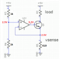
Beta for a typical transistor in the 1-10mA range is a minimum of 70-100, with a maximum of 300.
If you had a transistor that gave a beta of 100 at 4mA, the base current would be 40uA; so collector current would be 3.96mA. A 1% error. Is that close enough?
Beta for a typical transistor in the 1-10mA range is a minimum of 70-100, with a maximum of 300.
If you had a transistor that gave a beta of 100 at 4mA, the base current would be 40uA; so collector current would be 3.96mA. A 1% error. Is that close enough?