Your schematic is different from that of ScottWang in post n 4 in the connection between the NPN and PNP transistor. What are the pros and cons (if any) of your solution ?
Your schematic is different from that of ScottWang in post n 4 in the connection between the NPN and PNP transistor. What are the pros and cons (if any) of your solution ?
They are the same theories as another one can be modify from my circuit that it is to move the R3 to cross on the Vbe of Q2, the value should be change to 2.7k~10k.
No, I didn't, and I'm a bit surprised by your question. But, since you asked, it is not a complimentary symmetry emitter follower, and it is not an analog amplifier. It is a complimentary open collector output stage with two saturating switches of complimentary material polarity, just like a CMOS output (without getting all pissy about whether or not CMOS output transistors truly saturate) only with bipolar parts that can hard saturate. And just like the output stages of just about everything except the original 555 y'all love so much, there is cross-conduction protection. In this case it is in the form of a static DC bias path that has an "on" voltage which is greater than the power rail.
As for my folly, think. The maximum input voltage is 10 V and the pull down transistor has a 15 V zener in front of it. Without the cap, the lower device never comes on. Thus the output stage would have the same asymmetrical output impedance of the previously posted circuits. With the cap, the 10 Vp-p drive voltage centers itself between the power rail and GND in a few cycles. The drive voltage and current to each transistor now is identical, assuring a symmetrical output impedance. The series resistor and capacitor set the base current to insure saturation but not overdrive the output devices.
Notice in post #8 that after two saturated switches to radically quicken the output waveform edges compared to the input, the 24 V output still has a trailing edge that is slower than its leading edge. This is because both circuit stages are single-ended.
They are the same theories as another one can be modify from my circuit that it is to move the R3 to cross on the Vbe of Q2, the value should be change to 2.7k~10k.
From your post n. 4 it seems that the output current is load independent, as you calculate it as 10(Beta)*I_R4 (the RLoad is not shown in the formula).
Instead MikeML in post n. 22 said that the curreent load is 24V/RLoad = 24mA. As if the Beta of the output transistor is not relevant.
I am wrong in my considerations ?
The 24mA in the circuit of MikeML is also the false load, the real load is your input of device.
The current of output was limited by R4 in my curcuit, and I was setup about 50 mA, how much current it will draw that it will depends on the input of device.
I have a 24VDC supply, and a generator that outputs a 1KHz square wave with an amplitude of 10V referred to ground. How can i get a square wave of 24V amplitude (referred to ground) ? The signal will be loaded with 20 or 30 mA.
This implies that the driver be capable of switching on with a minimal voltage loss, and that it be capable of driving a R=E/I=24/0.03=800Ω load. I did the math in my head and estimated 1000Ω.
The circuit of post #8 shows a 1000Ω load resistor in the dashed box, clearly labeled "load". I worked out the other resistors so that the two transistors are operated as saturated switches, with a base drive current ~Ic/10. The high-side switch, Q1 will drive the load resistor to about (24V-Vcesat) = ~23.7V when on.
So the "/10" in your and ScottWang equations is not the transistor Beta, but the ratio of Ic and Ib that ensures that the transistor is in full saturation.
So the "/10" in your and ScottWang equations is not the transistor Beta, but the ratio of Ic and Ib that ensures that the transistor is in full saturation.
When we using the components to design the curcuit, we have to according the parameters of datasheet, you can go to check anyone of the transistor and look at the item of Vce(sat).
an analog amplifier will amplify a digital signal too. if you want a 50-50 duty cycle 1khz square wave, run a 2 khz square wave thorugh a cmos flip flop first, that will turn it into a 50-50 duty cycle 1 khz.
So the "/10" in your and ScottWang equations is not the transistor Beta, but the ratio of Ic and Ib that ensures that the transistor is in full saturation.
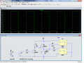
This is my first use of LTSpice, and try to simulate the behaviour of AnalogKid schema. From what explained from AnalogKid i expected to don't see the first two or three cycles of square waves in output, instead the simulator show also these cycles at the beginning of the simulation (first 10ms). Moreover i am surprised (but maybe a my error) to see the output level go up to 24V instead of (24V -VCEsat).
This is my first use of LTSpice, and try to simulate the behaviour of AnalogKid schema. From what explained from AnalogKid i expected to don't see the first two or three cycles of square waves in output, instead the simulator show also these cycles at the beginning of the simulation (first 10ms). Moreover i am surprised (but maybe a my error) to see the output level go up to 24V instead of (24V -VCEsat).
Although the analog amplifier can be amplifying the digital signal, but that is in the low frequency, some other day, if you meet the high frequency then it could be a problem, so doing this way is not a good way to learn the digital signal amplifier or digital voltage converter.
This is my first use of LTSpice, and try to simulate the behaviour of AnalogKid schema. From what explained from AnalogKid i expected to don't see the first two or three cycles of square waves in output, instead the simulator show also these cycles at the beginning of the simulation (first 10ms). Moreover i am surprised (but maybe a my error) to see the output level go up to 24V instead of (24V -VCEsat).
Your simulation looks fine. You are correct, the high output is 24 V - Vcesat, but Vcesat is less than 0.1 V, so it is hard to see on a 24 V scale. If you look at the voltage between R3 and C1, you will see a tilt in the waveform. This is due to the capacitor discharging as it drives the transistors. You can use this to calculate the minimum base current to make sure it is large enough for the load you are driving. Or, LTSIM can plot the current through R3 so you can see the result on the screen. Either way, you want the minimum base current to be around 0.05 or 0.1 times the load current to ensure transistor saturaion and a low Vcesat.
Your simulation looks fine. You are correct, the high output is 24 V - Vcesat, but Vcesat is less than 0.1 V, so it is hard to see on a 24 V scale. If you look at the voltage between R3 and C1, you will see a tilt in the waveform. This is due to the capacitor discharging as it drives the transistors. You can use this to calculate the minimum base current to make sure it is large enough for the load you are driving. Or, LTSIM can plot the current through R3 so you can see the result on the screen. Either way, you want the minimum base current to be around 0.05 or 0.1 times the load current to ensure transistor saturaion and a low Vcesat.
That might be a minor variation in the way your version and my version of LTSpice are configured. Your schematic is fine, and the circuit will work as indicated.
Since it is a PLC you are driving you may not like the AC coupled circuit. And since the PLC may be active high or active low it might be better to use some sort of push pull arraignment like this: That way the output voltage won't change depending on the load.
Since it is a PLC you are driving you may not like the AC coupled circuit. And since the PLC may be active high or active low it might be better to use some sort of push pull arraignment like this: That way the output voltage won't change depending on the load.
That might be a minor variation in the way your version and my version of LTSpice are configured. Your schematic is fine, and the circuit will work as indicated.
 Facebook
 Google
 GitHub
 Linkedin