1 second delay using logic circuit

Thread Starter

nailtherail

Joined Apr 28, 2019
6
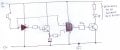
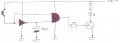
Hi,I am relatively new to this sort of thing but have been playing with logic circuits. I am trying to create a circuit that when a button is pressed, the LED lights for one second, no matter how long the button is pressed for. At present thought it would be easy to charge the capacitor via a 'NOT' gate, then when the button is pressed, the output from the not gate disappears but is still supplied for a short time from the capacitor. Both the button and capacitor have inputs to a 2 input 'AND' gate, if both inputs are high then the transistor turns on and lights the LED, until the capacitor has discharged!!
Seems simple enough I thought, but this circuit just keeps blowing the 'NOT' gate chip. Is there a better circuit or can anyone say what I am doing wrong!!
 

Attachments

Thread Starter

nailtherail

Joined Apr 28, 2019
6
hi ni,
Welcome to AAC,
What is the shortest possible time the switch will be pressed.?
E
The switch could be anything from mere touch/flick of a finger, to constantly being held down.. In real terms I would think that the button could be pressed for half a second or longer.
 
Last edited:

ericgibbs

Joined Jan 29, 2010
18,840
hi n,

A mere touch/flick of a finger is a subjective delay.o_O
Lets assume its 0.1S, so to charge a 100uF cap to approx one time constant would require a series 1k

So replace that short wire from the NOT to the 100uF with a 1K resistor, lets know how it goes.

E

EDIT:
Where did you find the circuit. is not going to work????
 
Last edited:

dl324

Joined Mar 30, 2015
16,909
Is there a better circuit
Here are some options that only use inverters, the arrows indicate trigger edge:
upload_2019-4-28_7-12-22.png
EDIT: The bottom circuits aren't suitable for what you want.

They're all retriggerable oneshots. If you want one that isn't retriggerable, you can use this:
upload_2019-4-28_7-11-17.png
EDIT: This circuit has an omission. Corrected below.

If you're concerned about power dissipation in the inverter with the R/C on it's input, you can use schmitt Schmitt inverters.
EDIT: This great man's name should be capitalized.

I am relatively new to this sort of thing but have been playing with logic circuits.
You should get in the habit of specifying component values and using component designators.
 
Last edited:

AnalogKid

Joined Aug 1, 2013
11,036
The circuit you want is called a monostable multivibrator, because the original form was a special case of the multivibrator circuit. To make the output completely independent of the input (once triggered) requires two things - a series capacitor (yours is shunt) and positive feedback. The classic form using logic gates has two NAND gates (for a negative-going trigger signal) or two NOR gates (for a positive-going trigger signal). Here is the NAND version:


It is similar to circuit #5 above, except that it uses another NAND gate as the inverter so you don't need two different IC packages for one circuit. Also, the 4081 should be a 4011.

In the rest state, Rt holes the U2 input low, which forces the U2 output high. This presents a high at one of the U1 inputs. The other input is held high by R1, so the U1 output is low. With a low on both sides of Ct, is has approx. 0 V across it.

When the input goes low, the U1 output goes high (basic NAND gate operation), which pulls Ct high. The voltage across a capacitor cannot change instantaneously (physics) so the U2 input is pulled high. This drives the U2 output low, and it is this low signal, fed back to the U1 input, that holds the circuit output low even when the input signal returns high. Now Ct starts to charge accept through Rt. Eventually the right side of Ct goes low enough to cross the U2 input transition level. This is the end of the timing period. U2 changes state to high, removing the low from the U1 input.

At this point there are two possible internal circuit actions, but neither one affects the output. IF the switch input still is low, the U1 output remains high. Ct continues to charge (down?) to 0 V through Rt. The output remains high, the timing pulse has ended, and the circuit just sits there waiting for the button to be released. When the button is released, U1 out goes low and Ct starts to discharge through Rt until both sides of the cap are at 0 V. IF the switch already is released when the output pulse ends and U2 out goes high, then U1 out goes low immediately and Ct starts to discharge.

At the end of the timing pulse, Ct drives the U2 input below GND, not a good thing. "B" series CMOS gates have a diode network on the inputs to protect them, but good practice is to add a signal diode in parallel with Rt to take the stress off of the gate. This has the added benefit of partly "shorting out" Rt for a much more rapid discharge of Ct. This shortens the time it takes to the circuit to reset itself so the next output pulse is the same as before.

Because of the slow charge/discharge edge into U2, that gate should be a Schmitt trigger part, such as a CD4093, rather than the standard CD4011 NAND gate.

ak
 

Thread Starter

nailtherail

Joined Apr 28, 2019
6
hi n,

A mere touch/flick of a finger is a subjective delay.o_O
Lets assume its 0.1S, so to charge a 100uF cap to approx one time constant would require a series 1k

So replace that short wire from the NOT to the 100uF with a 1K resistor, lets know how it goes.

E

EDIT:
Where did you find the circuit. is not going to work????
Having reconstructed the circuit to include the changes.
When the NOT gate input (pin 5) is 0v due to the button being O/C. On putting the probe on the NOT gate output (pin 6), it briefly shows 12v (and begins to drop, I presume because the capacitor is discharging through my meter), at 10v the LED lights!!! This is despite there being no input voltage as the switch is O/C. At about 5v the LED goes out!!
If I press the button, for either a long or short period, nothing makes the LED light, until I put the probe on (pin6 of the NOT gate).
 

danadak

Joined Mar 10, 2018
4,057
The reason you are blowing up your inverting gate, the large Cap current
charge and discharge thru its output.

upload_2019-4-28_12-2-32.png

Regards, Dana.
 

Thread Starter

nailtherail

Joined Apr 28, 2019
6

Attachments

AnalogKid

Joined Aug 1, 2013
11,036
Having reconstructed the circuit to include the changes.
When the NOT gate input (pin 5) is 0v due to the button being O/C. On putting the probe on the NOT gate output (pin 6), it briefly shows 12v (and begins to drop, I presume because the capacitor is discharging through my meter), at 10v the LED lights!!! This is despite there being no input voltage as the switch is O/C. At about 5v the LED goes out!!
If I press the button, for either a long or short period, nothing makes the LED light, until I put the probe on (pin6 of the NOT gate).
you don't say what the gate part number is; because of the +12 V supply, let's assume it is CMOS. There *must* be some kind of current limiter between the gate output, the capacitor, and either Vdd or GND. 100 uF is large enough to store damaging energy.

Separate from that, you must never leave a CMOS input floating. This can cause both erratic operation (which you are seeing) and physical damage to the part.

Please post an updated schematic. Use a reference designator for each component (R2, SW1, U1, etc.) so we can have a decent discussion.

Edit: just saw your latest schematic. The pin number assignments do not agree with standard logic components, particularly the power and GND pins. Also, there is no discharge path for the timing capacitor.

ak
 
Last edited:

danadak

Joined Mar 10, 2018
4,057
The other problem you have not using a Schmidt is slow rise/fall time signals
causing multiple transitions at the output of the circuit. In your case driving an LED,
you probably do not care. But good practice makes sure signals in digital circuits,
especially CMOS. have fast Tr and Tf times.

http://www.ti.com/lit/an/scba004d/scba004d.pdf


Regards, Dana.
 

dl324

Joined Mar 30, 2015
16,909
And the diff amp. And the follower. And chopper stabilization. AND - all with *jars* (empty-state devices).
In recognition of his accomplishments, we should at least try to spell his name correctly. For my part, I'll start capitalizing his name.
 
Top