URGENT HELP NEEDED: 555, transistor, monostable

Thread Starter

gunexer

Joined Mar 30, 2009
12
/* UPDATED */


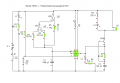
The circuit should work like this, upon turning on S1, L1 will be on and the circuit will be on standby. Once I press S2, the timing will be initiated and timing will begin (time is chosen by RS1 rotary switch). This will cause L2 to turn on. After the timing has been complete, L3 and B1 will be on for approx. 0.5 seconds.

This has worked in the Crocodile Clips simulation software.
However, when I tried it in real-life it did not work, the B1 and L3 were on right after I completed S1, and after I pressed S2, L3 turned off, L2 turned on, but B1 was still on. I tried S3 (Push to break) to no avail.
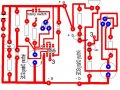
I have also attached the PCB diagram, could there be a problem there?

Moreover, my friend has the same transistor section in his circuit but it works fine for him.....

P.S I am using two circuit boards so the +a and +b seen in the PCB screenshot are merely wires linking them together.
 

Attachments

Last edited:

SgtWookie

Joined Jul 17, 2007
22,230
Going back and editing your first post after a half-dozen replies have been made can make those replies irrelevant; so I have removed all of my replies except this one.

Now that you've managed to get your schematics posted and have included reference designators, perhaps we can proceed.

What time intervals were you hoping to achieve with such a large capacitor (1,000uF) and such a broad range of resistance? (310k, 510k, 1MEG)

Take a look at National Semiconductor's datasheet for the LM555.
National's site: http://www.national.com - use the Search function.
It has a schematic of the IC's internals on page 1.
On the lower left of the diagram, you'll see pin 4, "Reset".
What does that pin connect to?
What do you think would be the best way to control that input?
 
Last edited:

Thread Starter

gunexer

Joined Mar 30, 2009
12
I don't think that we have to go over the RS1 - C1 part because if I recall correctly they should give me time delays of 5 minutes, 10 minutes and 15 minutes.

For the pin 4, I believe that it is the reset? and that it connects to the positive rail. Basically I just have a push-to-break there so that I can stop the timing.
 

Thread Starter

gunexer

Joined Mar 30, 2009
12
I believe that the First Half of the circuit (circuit up to the 3-output), is correct. I think that the problem lies in the second half, especially the transistor section.
 

SgtWookie

Joined Jul 17, 2007
22,230
I don't think that we have to go over the RS1 - C1 part because if I recall correctly they should give me time delays of 5 minutes, 10 minutes and 15 minutes.
I see.

For the pin 4, I believe that it is the reset? and that it connects to the positive rail. Basically I just have a push-to-break there so that I can stop the timing.
That's not going to work correctly.

Did you look at the datasheet from the National Semiconductor website? The schematic on page 1 of the LM555 timer datasheet, and what pin 4 (RESET) connects to internally?

What do you think would be the most simple manner of correcting your connections to pin 4 in order to make that feature function properly?

You know that since this is homework, we can't do it for you - but we can help you if you're stuck. Doing it for you would defeat the whole purpose; you wouldn't learn anything.

Also, your board layout does not have reference designators on it. If your software supports silkscreen layers, turn them on.
 

Thread Starter

gunexer

Joined Mar 30, 2009
12
Ok, I'll add the references to my board layout. I am pretty sure that the reset works as the majority of my class are using it. Unless....we're all wrong. In fact, I recall using the omega circuit set to test the reset function and seems to work.
 

Attachments

Wendy

Joined Mar 24, 2008
23,408
The reset works, but I don't see a signal conditioner on pin 2. Check my monostable experiment out, and compare notes.

555 Monostable

What is B1?

Looking at the schematic again, you need a pulldown on pin 4. This is digital logic, it doesn't assume states too well, a pulldown of 4.7KΩ or so will make sure the pin sees a true low when the button is pushed.
 
Last edited:

Thread Starter

gunexer

Joined Mar 30, 2009
12
Sorry I'm not very familiar with these terms, by signal conditioner you mean the trigger right? B1 = buzzer
 
Last edited:

Thread Starter

gunexer

Joined Mar 30, 2009
12
and can you take a look at the transistor section? some of my friends are using it and it works for them...I'm starting to think that my PCB may be wrong...even though I can't find the error.

as you will see in the attached image, my friend's circuit has the same transistor section and it works on his ACTUAL circuit as well.
 

Attachments

Last edited:

SgtWookie

Joined Jul 17, 2007
22,230
Ok, I'll add the references to my board layout.
Good. This is also a double-check for you.

I am pretty sure that the reset works as the majority of my class are using it. Unless....we're all wrong. In fact, I recall using the omega circuit set to test the reset function and seems to work.
Have you looked at the datasheet yet?

I'll suggest that either you have not, or you don't quite understand what the input does.

I will tell you that how it is currently wired in your schematic is not quite correct; something is missing.
What do you think is missing, and why?
[eta]
Here, I attached the 555 internal schematic for you.
 

Attachments

Last edited:

Thread Starter

gunexer

Joined Mar 30, 2009
12
I'm sorry, I don't know.....It's already the 3rd time that I've remade my circuit. I'm making it for my CW. Everytime my teacher says that it is correct and everytime I get a stupid mistake. I think it's the 5th pin...I hope it's not because if it is I will have to remake it again... Can you please see the other screenshot that I attached? THe one that my friend is using? How come it works for him?
 

SgtWookie

Joined Jul 17, 2007
22,230
Pin 4 (reset) needs a 2k to 10k resistor to ground to provide a current path for Q25's base.
Otherwise, it won't turn on.

When you push S3, it disconnects Vcc from pin 4. A resistor to ground will provide a current path from the base of Q25 to ground. When Q25 turns on, it sources current to the base of Q14, turning it on, which pulls the DISCHARGE pin 7 low.

Do you understand now?
 

SgtWookie

Joined Jul 17, 2007
22,230
Run your simulation, and look at the current flowing through the NPN transistor.

Do you notice a big spike in the base current when the 555 output goes low? Like 1 or 2 Amperes?

Has your teacher told you about limiting the current through the base of a transistor?
 

Thread Starter

gunexer

Joined Mar 30, 2009
12
Ok, I'm at my electronics class now :), I'm not really familiar with the 555-IC. I did take a look at the article but I didn't understand it fully. I'll take a look at it again.
 

Thread Starter

gunexer

Joined Mar 30, 2009
12
Ok, thanks for the help Bill and SgtWookie. I discussed this with my teacher and she with her colleagues and I was advised to replace S3 with a 10k resistor. This way the S3 can be connected to the 0V.
 

SgtWookie

Joined Jul 17, 2007
22,230
Ok, thanks for the help Bill and SgtWookie. I discussed this with my teacher and she with her colleagues and I was advised to replace S3 with a 10k resistor. This way the S3 can be connected to the 0V.
If S3 is a normally-closed switch, then the "fix" will not work correctly.
Pin 4 needs to be held high for normal operation, and pulled low for the reset function. If you make the proposed changes, you would release the switch to cause the timer to reset, and hold it down for normal operation.

S3 should remain as it was, connecting pin 4 to +9v.
A 10k resistor needs to be added from pin 4 to ground.

That way, when S3 is pushed, the 10k resistor will pull the base of Q25 to ground.
 
Top