
Hi guys,
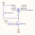
Attached is a schematic of a high side PMOS switch. The base of the transistor will actually be controlled by a microprocessor. The BJT is used to provide enough gate voltage to keep the PMOS off. When 3.3V is applied to the base, the BJT should send the gate signal to ground, turning on the fet.
Attached is the schematic.
PMOS datasheet:
http://www.fairchildsemi.com/ds/FD/FDS6681Z.pdf
BJT datasheet:
http://www.nxp.com/documents/data_sheet/MMBT3904.pdf
Any suggestions would be greatly appreciated. I am more of software guy.
Thanks!
Attachments
-
 65.5 KB Views: 111


