Re-biasing discrete bjt small signal preamp

Thread Starter

analog_audio

Joined May 27, 2024
8
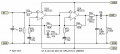
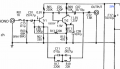
I came across this phono preamp which takes in small (~5mv) audio frequency signal from a turntable and amplifies it by ~38db.
The first stage transistor (TR1) is running at a very low Vce (1.5v or less). This places the Q point at the very fringe end of the vce-ice/ib curve almost near the knee of the curve. I believe this is not a very linear point of operation. My goal is to increase the Q point of this transistor just a little bit up to about 3v without altering the load impedances and gain in a big way.
Do note that the small RC network by itself at the bottom of the circuit is the riaa equalization network which is needed for a flat frequency response in a phono preamp. R13 also serves as some kind of feedback.
Would love to get the experts ideas and thoughts on this.
Thanks!
 

Attachments

Thread Starter

analog_audio

Joined May 27, 2024
8
Yes indeed I have seen that and actually I do have fully stuffed pcbs for a popular opamp diy phono pre that I will be taking on as the next project but what I like about this project/preamp is that its a basic building block type of circuit from which you can learn a lot, and it sounds quite good as is and I feel there is room for more improvement in this area so I am curious to find (and then compare with that opamp pre I need to boot up!).
Unfortunately my knowledge about multi-stage transistor amplifier design shows its limits for this type of stuff so I thought I'd ask here.
 

Thread Starter

analog_audio

Joined May 27, 2024
8
Strikingly similar. The last line about improving linearity and adjusting dc bias is what I am trying to do. Does the book have further comments on specifically what to change for "adjusting dc bias" ?
The biasing scheme is slightly different in the schematic I posted though. Any thoughts on what to change ? I was thinking decreasing R5 (first stage load R) to 100k and increasing R13 (dc feedback) to 440k as a starting point and see where things land.
 

Ian0

Joined Aug 7, 2020
10,277
Strikingly similar. The last line about improving linearity and adjusting dc bias is what I am trying to do. Does the book have further comments on specifically what to change for "adjusting dc bias" ?
Unfortunately not. It's just part of a section on the history.
The biasing scheme is slightly different in the schematic I posted though. Any thoughts on what to change ? I was thinking decreasing R5 (first stage load R) to 100k and increasing R13 (dc feedback) to 440k as a starting point and see where things land.
If you reduce R5, it will reduce the gain of the first stage.
R13 provides the base current for Q1. if you increase R13, it will reduce the voltage at the base of Q1.
It would seem that the first stage runs at a collector current of 100uA, which is probably about right for the best noise performance of Q1.

The operating point depends on the voltage across R7, which is rather too dependent on the exact voltage of Vbe of Q1 (which varies with temperature) and the tolerances of R11 and R15.
To get a sensible voltage on the collector of Q1, you need to reduce its collector current, for which you have to reduce R15 by quite a small amount.
I would suggest connecting larger values in parallel with it until you get it about right.
As Q1's collector current reduces, the collector voltage will increase, which will put more current through R11 and R15 which increases Q1's bias, increasing its collector current.
This is a SPICE simulator of Self's circuit:
Screenshot from 2024-05-28 21-24-47.png
 

Thread Starter

analog_audio

Joined May 27, 2024
8
..
To get a sensible voltage on the collector of Q1, you need to reduce its collector current,
..
Question - What would happen if only R7 was slightly increased instead ? R7 is Re of Q1. I understand that could drop the gain of that stage but wouldn't that decrease Ic of Q1 too ?
I feel like Ib of q1 is already quite low - probably in the 10-20ua range so instead of reducing Ib further I am thinking of achieving this by reducing Ic directly. Thoughts ?
 

Bordodynov

Joined May 20, 2015
3,188
Question - What would happen if only R7 was slightly increased instead ? R7 is Re of Q1. I understand that could drop the gain of that stage but wouldn't that decrease Ic of Q1 too ?
I feel like Ib of q1 is already quite low - probably in the 10-20ua range so instead of reducing Ib further I am thinking of achieving this by reducing Ic directly. Thoughts ?
You don't know very well the limits of allowable voltages in the amplifier mode. The transistor works perfectly well even at zero base-collector voltage. Also, to reduce noise they try to reduce the collector voltage. Raising the voltage will not reduce distortion, but will increase the noise level of the first transistor. The leakage of the transistor starts to grow after the voltage Uce>1 V, which leads to additional noise.
 

Thread Starter

analog_audio

Joined May 27, 2024
8
Here is a typical Vce-Ice/Ib curve of a transistor. See the "knee" of the curve towards the far left ? especially for low Ib of 10-20ua. Its highly non-linear (in other words high distortion). You dont want an audio amplifier operating in that region. Might work for an on-off switch application but not for audio.
If I was to design my audio amplifier I would not choose an operating point below 3V. In the circuit I posted in my original post Q1 operates at about 1.6V and I am trying to increase that.

Screenshot 2024-06-05 at 7.31.25 AM.png
 

crutschow

Joined Mar 14, 2008
34,894
Ian0's circuit sim in post #6 shows a Q1 collector voltage of about 3V, and an emitter current of about 47mA.
Isn't that what you want?
 

Thread Starter

analog_audio

Joined May 27, 2024
8
indeed a great reference, but what I want to do is just want to make a small modification to the unit I already have with the original circuit, not build a new one from scratch.
Thanks.
 

Ian0

Joined Aug 7, 2020
10,277
. Also, to reduce noise they try to reduce the collector voltage. Raising the voltage will not reduce distortion, but will increase the noise level of the first transistor. The leakage of the transistor starts to grow after the voltage Uce>1 V, which leads to additional noise.
Could you elaborate? if there is already collector current flowing (as Vce<V supply) what leakage are you referring to? And what is the mechanism by which it makes noise? Schottky noise?
 

Bordodynov

Joined May 20, 2015
3,188
Could you elaborate? if there is already collector current flowing (as Vce<V supply) what leakage are you referring to? And what is the mechanism by which it makes noise? Schottky noise?
In addition to semiconductor structure currents, there are ionic conduction currents across the crystal surface. I had a batch of KT361 transistors with increased leakage. I found that the additional current occurred at voltages greater than 1 V and its voltage dependence was proportional to the square root of the voltage. This character of conductivity (presence of a voltage threshold) is characteristic of electrolytes.
Any excess current increases noise!
Spice models do not simulate the current considered.
Perhaps this current due to dirt on the surface is not characteristic of modern transistors. But the circuits considered here were developed a long time ago, and the choice of low voltages on the input transistor was relevant then.
 

Thread Starter

analog_audio

Joined May 27, 2024
8
Have you found that to be the case with any other bjt or just the kt361 ?
If it matters - the transistors in this phono preamp are from the late 70s and they are specifically characterized as "low noise small signal amplifier" and reasonably linear for audio. and made by reputed brands like Sanyo, Hitachi, RCA , TI, ..

Manufacturer and general part quality might have some implication as well ? KT361 seems to be just a general purpose transistor with no brand name, the only thing I could find was an odd looking datasheet in russian language. Are you sure that batch wasnt counterfeit ?
 

Danko

Joined Nov 22, 2017
1,858
Noise in transistor 2N2222:
https://www.onsemi.com/pdf/datasheet/p2n2222a-d.pdf
1717689562755.png
= = = = = = = = = = = = = = = = = = = = = = = = = = = = = = =
Noise in transistor 2C2545, 2C2546, 2C2547:
https://www.renesas.com/us/en/document/dst/2sc2545-2sc2546-2sc2547-datasheet
1717701418392.png
= = = = = = = = = = = = = = = = = = = = = = = = = = = = = = =
See PDF in attachment:
"3.2. Bipolar Junction Transistor (BJT) Noises, presenting in a BJT in active region:
•Shot noise generated by the collector current. Minority carriers, which enter from emitter in the base diffuse across the base until they reach the collector-base junction, where they are swept to the collector. The collector current IC consists of series of random current pulses and thus it shows a full shot noise. This noise is given by formula (9).
•Shot noise generated by the base current. The base current is due to 1) the recombination in the base and in the base-emitter depletion region; 2) the carrier injection from the base into the emitter. The both parts are independent random processes, which is perceived as a shot noise. It is included in formula (10).
•Thermal noise generated in the base resistor rb . rb represents the ohmic resistance of the base region. It is given by formula (8).
•Thermal noise generated in the resistor rc of the collector region. It is in series with highimpedance collector node and is negligible (see Fig. 12).
•Flicker and burst noise. Experimentally they have been found to be represented by current sources across the internal base-emitter junction. Usually they are combined with the shot noise of the base current in a single source ib 2 . They are included in formula (10). All noise sources in Fig. 12 are independent of each other, since they arise from separate, physically independent mechanisms."
 

Attachments

Last edited:

Bordodynov

Joined May 20, 2015
3,188
These transistors turned out to be "outstanding" in leakage current, but they met the technical requirements. I took the BC147 transistor. Its leakage can reach 15 nA (typical value is 0.2 nA).
And I showed the leakage of the transistor without leaks in the simulation.
The comparison shows that this good transistor also has leaks, but of course a thousand times less than the KT361.
leak.png
 
Last edited:
Top