One P-Channel High Voltage Mosfet is the Pass element on a 50-200V DC/400 mA linear power supply.

Thread Starter

Ioannis66

Joined Nov 7, 2012
45
I have a similar issue. One P-Channel High Voltage Mosfet is the Pass element on a 50-200V DC linear power supply. The needed current is about 400mA but seems that most devices have a SOA very much limited in the higher voltage operation. That leads to destruction of the Mosfet if current is over 300mA or so.

The Mosfet is working in linear region and was thinking to parallel 2 of them. But do they need large balancing resistors?

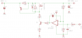
Parts I test are FQP4P40. I attach the circuit I am testing.


Mods Note:
Please don't hijack other member's thread.
This thread was split from Parallel mosfets or IGBT from single mosfet driver, if big enough?
 

Attachments

danadak

Joined Mar 10, 2018
4,057
Seems like a spice sim varying their threshold might be easiest
way to get at acceptable current sharing vs ballast R value.

Just do the MOSFETs one gate driven by a swept V source, the
other at some fixed current level to get a locus or results.

Regards, Dana.
 

ScottWang

Joined Aug 23, 2012
7,398
The Vgs of FQP4P40 is -10V, so Zd1 using 8.2V is too small that it can be use more higher to 12V~20V, R4 connected to Ground directly, concerning the Zd1 has a good stable voltage, I_Zd1 >=5 mA, R2(22K) change to 43K, R3(1K) change to 3.3K~4.7K.
 

Bordodynov

Joined May 20, 2015
3,179
Here's an idea for you. See how the regulating transistor and short-circuit protection are made. Instead of a reference voltage chip, use your opamp. Instead of the DN2540, use a conventional high-voltage field-effect transistor (gate to 5V supply). Operational amplifier through the resistor connect to the source. Then you will have not three inverting cascades, but only one. And the parameters will be much better.
2018-07-20_16-20-47.png
 

Thread Starter

Ioannis66

Joined Nov 7, 2012
45
Sorry for the hijack.

Thank you all for the replies and suggestions.

Regarding the selection of the 8v2 zener, it is indeed very conservative in relation to Vgs, but works OK so far. OK,will change to a higher one.

Ioannis
 

Thread Starter

Ioannis66

Joined Nov 7, 2012
45
If R4 is zeroed the stability seems to be lost. The selection was done based on the resulting max current through T1 of 5mA and the less heat dissipation on the resistor parts and T1 too.

Maybe having a bypass in parallel with R4 will help the noise in Vout. But grounding the T1 increases Vout instability.

I got access to a PS of such high voltage application that had two SCR's in the rectification . Attached is the circuit. The zener D7 reduces the voltage drop across the pass element and keeps it under control in regard with the output voltage.

Have not tested yet as it needs a sensitive SCR of the 0,1-0,5 mA gate current. Expecting to receive them this week.

Ioannis
 

Attachments

Bordodynov

Joined May 20, 2015
3,179
The Vgs of FQP4P40 is -10V, so Zd1 using 8.2V is too small that it can be use more higher to 12V~20V, R4 connected to Ground directly, concerning the Zd1 has a good stable voltage, I_Zd1 >=5 mA, R2(22K) change to 43K, R3(1K) change to 3.3K~4.7K.
The suggestion to replace the zener diode with a higher voltage does not make sense! The transistor operates in an amplification mode and there is no need to limit the gate-source voltage limit value. Look at the datasheet. It follows that even at a voltage of 5.5 volts the current exceeds 1 ampere. Therefore, the transistor will work with sufficient margin to control the drain current when using a zener diode (with allowance for the transistor threshold voltage fluctuation) at a voltage of 6.8 volts.
PS.
For switching (switching) stabilizers, I strongly support the recommendation of increasing the voltage of a zener diode, since. efficiency depends on this!
 

ScottWang

Joined Aug 23, 2012
7,398
If R4 is zeroed the stability seems to be lost.
My original thought was that you were used the pure pwm square wave, but it wasn't, so just keep R4.

Maybe you could try to in parallel an 1N4148 diode with R7, R7 just take care the discharge and depends on the frequency to adjust the values of R7 and C4.
 

ebp

Joined Feb 8, 2018
2,332
Using FETs intended for switching in linear mode at high voltage is always risky at higher voltages. They often simply will not survive because there are circumstances where sharing between the multitude of internal paralleled cells is poor, with some cells taking most of the current and failing as a result.. There are power FETs made specifically for linear applications such as the depletion mode device in Bordodynov's circuit. IXYS is one of the few companies that makes power MOSFETs for linear applications. They have a reasonable range of N-channel enhancement types. I don't know what they offer for P-channel or for depletion-mode devices. The types I've looked at are considerably more expensive than switching types of similar ratings.
 

Thread Starter

Ioannis66

Joined Nov 7, 2012
45
Not many offers of P-channel mosfet in general and especially for linear operation.

The most important detail is in the SOA curve, where a 10 or even 20A Mosfet is unable to handle 1A or less, at 300Volts.

This is my main problem. The circuit works just fine regarding control and regulation but cannot be Short circuit protected yet.

The circuit with the Thyristors is a nice idea and I am looking forward to testing it. Maybe on 25th the parts will be here to test.

@ Bordodynov and ScottWang:
The circuit is not a switching and works just like a classic linear regulator. Only the reference voltage is derived from my MCU PWM output and then filtered with the R7/C4 low pas circuit to give an analog reference voltage. Then the op-amp takes care the rest of the loop.

Ioannis
 

ScottWang

Joined Aug 23, 2012
7,398
The suggestion to replace the zener diode with a higher voltage does not make sense! The transistor operates in an amplification mode and there is no need to limit the gate-source voltage limit value. Look at the datasheet.
Vgss (Gate-Source Voltage) = ± 30, if the Vgs out of the range then the MOSFET still could be damaged.
 

ebp

Joined Feb 8, 2018
2,332
I thought I had looked at the datasheet for the FET, but I guess I didn't - probably thinking of another of the numerous FET-related threads.

Since the SOA curves include one for DC, I would certainly feel entitled to use it in linear mode. Regrettably, there aren't any numbers on the curves to go with the three numbered notes. I'm assuming the DC curve gets the 25°C case temp note, which means that SOA curve needs derating in any practical circuit.

I can't recall ever seeing anything on paralleling power FETs in linear applications. With such a large input to output differential, if I were to try it I would be inclined to use ballast resistors for at least two or three volts at a current low enough that a single FET would be in its DC SOA. Reasonably close matching of threshold voltage might be worthwhile and would probably allow lower ballasting voltage. I'd definitely keep the paralleled FETs at the same temperature as far as possible. With two FETs I'd put them side-by-side or even back-to-back on opposite sides on a symmetric heatsink. By the time you apply temperature derating to the DC SOA, two in parallel is probably marginal if short-circuit survival is required.

Because you have lots of input to output voltage differential, operating an N-channel as a source-follower should be quite workable and will give you more choices for FETs. But it changes the whole circuit.
 

Thread Starter

Ioannis66

Joined Nov 7, 2012
45
Because of the large in-out voltage difference I am now thinking very positive for the SCR circuit posted above. It reduces the in-out a lot, keeping theoretically the drop on the pass Mosfet around 70-80 volts. Well within a good SOA.

Ioannis
 
Top