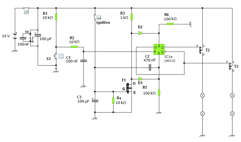
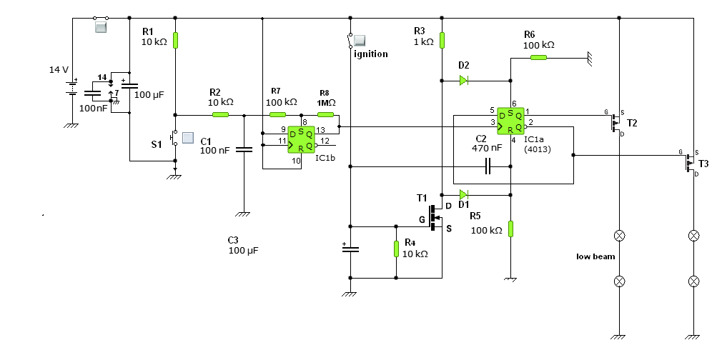
oh yeh.You already are using CMOS gates. .... the inverter and the and gates.
yes i did and that works. BUt i want to try and get my one to work, and his looks very complicated?did you unzip the example file that Jony130 so kindly gave you?
On edit:
What project are you working on where you have 260W and 200W 14V lights?
If you want supply CMOS gate in yenka you must use power connector from power supplies folder.
yes, but i dont understand what that means? if you haven't read this post from the start i am a "beginner".Jony130 already told you why the components blew up in post #17
Well I was thought about thisyes, but i dont understand what that means? if you haven't read this post from the start i am a "beginner".
What do i do with the "power connector ", and where do i connect it?
Ok i tryed that, not only do the same things blow up, but now the switch blows up. I put it in the same place as the diagram.Well I was thought about this
yep, no-problemIf i upload my circuit from yenka, could you or someone who has it, have a fiddle with it and see if they can get it to work?
ok thanks, its attached to this comment.yep, no-problem
The Cmos logic ICs will overheat if you do not properly disable the unused ones. Disable them by connecting unused inputs to ground.inverter and 2 AND gates keep blowing up?? why is that??
do you mean connect the 'S' pin of the flip flop to the negative?The Cmos logic ICs will overheat if you do not properly disable the unused ones. Disable them by connecting unused inputs to ground.
The S and R pins of a CD4013 must be grounded for it to work. All the inputs on the unused flip-flop should be connected to ground or to the positive supply.do you mean connect the 'S' pin of the flip flop to the negative?
If so, i tried that, and it does nothing. still blows up.
im sorry but i dont understand much of what you said. Why would the 'R' pin be grounded? isnt that where the power is supposed to come from?The S and R pins of a CD4013 must be grounded for it to work. All the inputs on the unused flip-flop should be connected to ground or to the positive supply.
Yenka is designed for old fashioned 5V TTL logic ICs that blow up when the supply is as high as 14V. You must use the "power connector" somehow to power the Cmos logic ICs with 14V.
No, i am using the CD4013, if you check my more recent circuit post you'll see i changed it. But still, it's design is exactly the same. And like i said, isn't R pin the input power and then S pin for negative? because both Q's are output and are for the lights, and the clock is connected to negative with a positive push switch to swap from high to low.Sorry. You are using a 74HC74 dual flip-flop which is completely different to a CD4013 dual flip-flop that I thought you had. The 74HC74 has a max allowed supply voltage of only 6V.
Its unused half must be properly disabled and its unused pins must connect properly to ground or to the supply voltage so that it performs the functions you want.
After adding the pullup resistor on the CD4013 and a pullup on the 555 trig, the circuit works somewhat normally. However, you have not expressed what the desired outcome should be. I know what it is, but what is unknown is your specifications. You have been secretative about those specifications.I need someone to figure out why the inverter and AND gates are blowing up, because i have no idea, and unless i figure it out i cant test my circuit because they are holding me back at the moment.
Why do you say that?Jony,
the thumbnails are difficult, at best to read. why not just upload the original graphic to the forum?
by Jake Hertz
by Duane Benson
by Jake Hertz