MOS - delay for time off

Thread Starter

adinellu

Joined Jul 27, 2015
5
Hello,

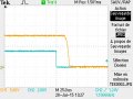
I have 4 square signals generated with a MSP, so with the logic level 0-3.3V. I need this signals with the logic levels 0-15V. I made a circuit like in the image attached. I used for the NMOS : NDS331N from Fairchild Semiconductor (1.3A, 20V) and for the PMOS : NTR4502PT1G from On Semiconductor (-1.95A, -30V). The switch ON is good, with no delay, but the switch OFF is taking ~25us. I tried to change the 2 pull-down but the switch OFF is always 25-30us. My signals have to be precise at less than us, because I have some signals with a time ON of 2us. See the attached photos for an example of my problem. Do you have any idea from where the delay appears from?

Thanks,
Adina
 

Attachments

Alec_t

Joined Sep 17, 2013
14,314
Do you have any idea from where the delay appears from?
It's due to the gate capacitance charge time via R2. R2 could be reduced, but ideally should be replaced by an active pull-up device.

Edit: You'd get a faster response by using BJTs instead of MOSFETs.
 
Last edited:

Thread Starter

adinellu

Joined Jul 27, 2015
5
Thank you, I tried with a 400ohm and the delay was reduced to ~1us. I will look into the solution with the BJTs.

Thanks again
 

crutschow

Joined Mar 14, 2008
34,452
Some BJT's have a significant turn-off (storage) delay but for those designed for switching, such as the 2N2369, this delay is quite small.

What is the load you are driving?
Why did you use such an odd value for the resistors?
Why did you use two MOSFETs?
What is the part number for the MOSFET?
 

Thread Starter

adinellu

Joined Jul 27, 2015
5
I wanted to use the standard value for the resistors, 10k, but we didn't have it, so I choose the next closest value I found in the lab. I didn't realised the value will have such a big impact on my circuit. I am not really at ease with the analog electronics. I am doing this signals to test an FPGA program I developped. The load will have 100mA max.
 

AnalogKid

Joined Aug 1, 2013
11,048
Just to be clear, let me restate the project. You have an input logic signal, 0V to +3.3V, and you want an output signal of 0V to +15V that can source and sink 100 mA, and has rise and fall times of less than 1 us. Is that correct?

If yes, a while ago I posted a voltage shifting driver circuit, and I think a variation of it will work for you.

ak
 

crutschow

Joined Mar 14, 2008
34,452
Below is the LTspice simulation of a circuit using 3 MOSFETs in a push-pull output to get fast rise and fall times.
I didn't have the models for your exact devices, but used ones that have similar characteristics, so your results with the actual parts should be reasonably close to the simulation.
The delay/rise-time/fall-time from input to output is less than 0.2μs.
R2 is to limit the shoot-through current during the switching transient.

Driver.GIF
 

Attachments

Thread Starter

adinellu

Joined Jul 27, 2015
5
AnalogKid yes, that is my project. I looked into your history but I found nothing about a voltage shifting driver circuit altough I found some pretty interesting posts.
Crutschow, thanks for your circuit, I suppose the 3rd MOSFET is the active pull-up device Alec_t was talking about?
 
Top