Logic gates(Schematics)

Thread Starter

Zanac-X

Joined Dec 23, 2011
51
hello everyone :)

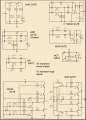
my project is to assemble all the gate circuits in one pcb but using only the fundamental components (resisters diodes etc) and i was wondering (using my attachment pic) :

1- is there any other circuit that is simpler and/or more economic/higher "η" ?
2-can i make my schematic design more compacted (im having trouble with the XNOR and XOR gates)

my ultimate goal is to have the perfect sheet that can help any student to understand the fundamental of logic gates and how it can be connected to give complex logic circuits

thanks very much for helping
 

Attachments

Thread Starter

Zanac-X

Joined Dec 23, 2011
51
awesome :D

thanks for the pic that was a lot of help now all i need is to simulate it ;)

about the power sources i know it represents the same point but i kept it that way so that it can explain how the circuit works or because it will give a more compacted circuit design without using (from-to) points
 

DickCappels

Joined Aug 21, 2008
10,169
Further, try to make your schematic representations more conventions. Put the most positive potential at the top of the schematic, use a ground symbol and consistently show signal flow from left-to-right. Draw the inverting transistors with the emitter grounded and the base connection going to the left. That will go a long way toward making this more readable.

In my own opinion, it would be best to not show the inputs connected to the power supply or ground, but left "floating" so the reader can more easily imagine what effect having each input high or low would have on the output.

Looks like a fun project.
 

Thread Starter

Zanac-X

Joined Dec 23, 2011
51
Thanks very much i will gladly fallow your advice now that you have mention it,it is easier to make the input signals flouting.but now that i have simulated it my circuits need a ground even if i make it a floating point in a real pcb the thing is when representing logic zero the circuit can not function without ground connected to the source representing the input signal, and the floating point(power rail) only have one pin so now im asking :

im i missing something here because im assuming that when i turn of the switch to give a logic zero im just connecting to ground right ?

sorry for troubling you and thanks very much :)
 

WBahn

Joined Mar 31, 2012
30,045
You don't indicate where your output of each circuit is. Since you are saying that the point is to make it easy for students can use these to build up more complex logic circuits, it is important that they see how they are supposed to connect these together.

For instance, how would someone take your circuit for an OR gate and your circuit for a NOT gate and put them together to form a 2-input NOR gate?

You gates have switches as input and photons as output. But to be useful to interface together, you need to have compatible inputs and outputs.
 

LDC3

Joined Apr 27, 2013
924
Thanks very much i will gladly fallow your advice now that you have mention it,it is easier to make the input signals flouting.but now that i have simulated it my circuits need a ground even if i make it a floating point in a real pcb the thing is when representing logic zero the circuit can not function without ground connected to the source representing the input signal, and the floating point(power rail) only have one pin so now im asking :

im i missing something here because im assuming that when i turn of the switch to give a logic zero im just connecting to ground right ?
If you still want to use switches as the input, you can use a SPDT switch and have one pole connected to Vcc and the other to ground. The common will be the signal into the circuit.
 

Thread Starter

Zanac-X

Joined Dec 23, 2011
51
thank you all for everything :D :

this is the last update to my sheet, although I've found a way to simulate the circuit using signals instead of sources but i kept it as it is to give students the ability to fallow the circulation of current in each circuit

thank you very much for your help and i'll be glad if you can help me with making it even more compacted .

Zanac-X
 

Attachments

panic mode

Joined Oct 10, 2011
2,740
no, that is terrible idea... you do not want to put switches in parallel with voltage sources - ever!
also the XOR gate circuit is wrong, you switched emitter and collector
 

Thread Starter

Zanac-X

Joined Dec 23, 2011
51
thanks for telling me but may i ask why not to connect a switch parallel to a source as my simulation is done as in real life with explosion happening if something is wrong so............

also i did not get correct results until i flipped the transistors maybe you should try to simulate it and see if something is wrong :)

im using circuit wizard as a simulator
 

panic mode

Joined Oct 10, 2011
2,740
just use simulation to measure current through switch and try to estimate suitable wire size... since you are college student (dept. of electrical power) ask your professors for assistance. i'd love to see their faces when they see the circuit. :-D

as for simulation - i do not need one as this can easily be calculated in head (at least for simple circuits and this one is a no-brainer):

we are dealing with digital circuits so transistors are expected to operate as switches.

you have 5V and 9V sources.

main current through transistors is collector-emitter (base current is much smaller and neglected).

to light up LED you have to get it' cathode to potential lower than anode (lower than 9V - Vf).

the way you drew it, that lower potential is +5V. so if either transistor conducts we get 9V-5V = 4V across LED and it's resistor. if LEDs Vf=2.3V then LD current is
(4V-2.3V)/220 Ohm = 7.7mA which is ok.

but for this to work, (and you are using NPN transistors) emitter would have to be on lower potential than collector. but since collector is at 5V and emitter can only be between 5V and 9V this is impossible.

i do not need simulator for such trivial things. note BJTs also have beta in reverse but it is much smaller than forward beta. suppose forward beta is 100 and reverse beta is 5.

then if you had transistors in normal orientation, Ib = (5V - 0.7V)/10k = 0.43mA
and Ic= 100*Ib = 43mA. But this cannot happen since Ic is limited by LED and resistor to 7.7mA so transistor is in saturation (good).

but if transistor is in reverse (as you have shown) then we must use reverse beta so Ic=5*Ib=2.1mA and since 2.1mA<7.7mA transistor is not in saturation (not working as a switch).

normal LEDs are rated for 20mA but 10mA will be just fine. 7.7mA will still look ok but 2.1mA will be very dim.

with slight modification (for example using spdt buttons on inputs and 5V supply), you would get almost 5V across LED and resistor and some 12mA. if you stick with 9V then LED current would go to 30mA and we don't want that in continuous mode.
 

WBahn

Joined Mar 31, 2012
30,045
note, if you do not plan on using inputs and outputs on gates then all of these circuits can be much simpler!!!
But he IS planning on this, otherwise it defeats his stated purpose from his original post: "my ultimate goal is to have the perfect sheet that can help any student to understand the fundamental of logic gates and how it can be connected to give complex logic circuits."
 

WBahn

Joined Mar 31, 2012
30,045
thanks for telling me but may i ask why not to connect a switch parallel to a source as my simulation is done as in real life with explosion happening if something is wrong so............
Would you ever take a metal wrench and short the terminals of your car battery?

Hopefully the answer is no.

Shorting a voltage source results in the largest current that the source is capable of producing, being limited only by the intermal resistance (or limiting circuitry) of the source. For many sources, even small batteries, that current can be high enough to dissipate enough power to result in a fire or an explosion (many batteries give off hydrogen gas as a normal byproduct of operation and the higher the current the faster the gas is given off).
 

Thread Starter

Zanac-X

Joined Dec 23, 2011
51
since you are college student (dept. of electrical power) ask your professors for assistance. i'd love to see their faces when they see the circuit. :-D
:D fair enugh.....you have all the right to say that but let me explain :

1st : thank you very much for your help it really means a lot :)

2nd : we dont have "professors" we have teachers whom i like to call "copy cats" as they just copy pages from the first book they see and just repeat some fancy words so that they can sound awesome (and one time a teacher said that we can connect a negative resistance [as in real resistor] to balance a Y-connected load)

long story short i live in a contry that just wont admit that you are right and if i showed it to my "teachers" they will not get whats in the sheet (i did really try that with some old pojects) and they will say one of two things :

1-good good excellent keep up the good work :rolleyes:
2-wrong go simulate it again :mad:

so im really trying to catch up with what im supposed to study thats why im studying the chapters of this site

so now i hope you can understand the level that im at (im trying to become a real electrical power engineer on my own) and im really sorry if im asking silly Qs :)

3rd : with what you have said (which no makes me feel better about what ive done, i will try to fix it

thank you very much for the explain
 

Thread Starter

Zanac-X

Joined Dec 23, 2011
51
panic mode : of course,now that you have explained whats going on (which is just what i needed) now i can work properly

and yes i was thinking of using SPDT switches but i thought im just Exaggerating and i just needed a normal switch to get the job done

thank you very much im really glad for the help
 

Thread Starter

Zanac-X

Joined Dec 23, 2011
51
Shorting a voltage source results in the largest current that the source is capable of producing
WBahn : ok now i admit........im an idiot..........i know that but i just didnt see it.

thanks for telling me
 

WBahn

Joined Mar 31, 2012
30,045
Not necessarily an idiot. You are asking the questions, which shows you want to learn. Like everyone, as you learn about A and learn about B, you tend to put the pieces together a bit at a time and so don't see how A and B relate to each other right away. Sometimes the connection becomes apparent on its own, and other times it needs to be pointed out. As an engineer the first thing that you need to be able to do is to ask the right questions, only then can you start finding the answers.
 
Last edited:

WBahn

Joined Mar 31, 2012
30,045
i think its done........how about you guys ?
But, as I said a long time ago, if your goal is to show how simple gates can be used to build complext logic circuits, how do these circuits accomplish that? How do you connect these gates together? Your inputs are switches and your outputs are LEDs.
 
Top