I made my first 3 stage Amplifier.

Thread Starter

babaliaris

Joined Nov 19, 2019
208

I did not make any mistakes building it, but there is a lot of distortion and the reason is probably that the components do not "sit" well enough in the breadboard holes. The distortion volume/gain does not change when I adjust the volume in my smartphone, it always sounds quite loud.

I also do not have an oscilloscope to see which stage messes with the signal.

I was checking stage by stage the DC Operational Point with my two multimeters, as I was building it and everything seemed ok. Also I did a last check at the end.

Probably the sound vibrations might have caused a lot of components to jump at the vibration frequencies, which might lead to unstable connections and thus distortion.

LTSpice Project in the attachments.

Smartphone App Image.jpg

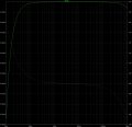
Frequency Response.jpg

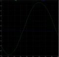
Transient Simulation.jpg
 

Attachments

Last edited by a moderator:
Probably ripple of power supply. You can increase Vcc filtration by adding the capacity or use a linear regulator.

But worst, you have load connected as inverter. This pick up a lot of noise. I would connect load to Vcc rail, not Gnd.
 

Thread Starter

babaliaris

Joined Nov 19, 2019
208
Probably ripple of power supply. You can increase Vcc filtration by adding the capacity or use a linear regulator.
I should have thought of that, it is a good idea to use a cap in parallel to the VCC input just to be sure.

But worst, you have load connected as inverter. This pick up a lot of noise. I would connect load to Vcc rail, not Gnd.
I don't have any knowledge about that.

Should I connect the speaker from the Amp output to + VCC? How can a speaker work as an inverter? I would like to know that.

Edited:
I've also found something about ground loops. I used 4 different isolated breadboard ground lines which I connected together using wires. The first for the power supply alone. Second above the transistors. Third below the transistors. And fourth down at the breadboard for the LEDs.
 
Last edited:
First bjt inverts the phase since you take signal from collector. Then every other stage doesn’t invert.
Connecting speaker according this the speaker is in phase with input signal.
IMG_0793.jpeg
Btw, the cap on input of amp doesn’t have to be so big like 4m7. A 220u should be sufficient for such a input impedance.
 

Thread Starter

babaliaris

Joined Nov 19, 2019
208
Btw, the cap on input of amp doesn’t have to be so big like 4m7. A 220u should be sufficient for such a input impedance.
The input impedance of the first stage (common emitter) is about 3kΩ. Do I calculate the value of the capacitor based on that impedance? So If I use a 220u then:

\[ Z_{C} = \frac{1}{2 \cdot \pi \cdot 20 \cdot 220 \times 10^{-6}} = 36.17Ω \]

Which is much smaller than 3kΩ.

Edited:
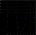
This is what I'm taking as a result of LTSpice when connecting the load to VCC:
Screenshot 2024-05-30 235133.png
 
Last edited:

BobTPH

Joined Jun 5, 2013
9,346
The distortion volume/gain does not change when I adjust the volume in my smartphone, it always sounds quite loud.
That sounds like noise, not distortion. They are quite different things. Do you hear this when there in no input signal (volume of phone all the way down?) What does it sound like?
 

Thread Starter

babaliaris

Joined Nov 19, 2019
208
The cross over distortion is visible on the scope trace. I imagine the THD must be quite high.
View attachment 323562
Do these harmonics come from the smartphone output? So I should create a good band filter to keep only the frequencies between 20Hz-20kHz?

That sounds like noise, not distortion. They are quite different things. Do you hear this when there in no input signal (volume of phone all the way down?) What does it sound like?
It was quite random actually. Sometimes turning the volume all the way down would completely stop any sound coming out from the speaker, sometimes I would hear a constant frequency beat.

Edited: By the way I found out that my big breadboard is actually really bad quality in terms of the spring attachments in the holes. When you place a resistor, for example, it does not tighten it and it causes it to "swim" inside the breadboard's holes. This is definitely one problem.
 

Dave Lowther

Joined Sep 8, 2016
263
Do these harmonics come from the smartphone output?
I think the waveforms in your opening post are a simulation. If I've understood that correctly then the distortion isn't coming from your smart phone. I assume the simulator produces an ideal sine wave.

If you don't know anything about cross over distortion see https://en.wikipedia.org/wiki/Crossover_distortion

You can never get rid of cross over distortion using class B, or class A-B, but you can minimise it. If you can see a kink where it crosses 0V on a scope trace then that's going to be quite high THD.
 

Ian0

Joined Aug 7, 2020
10,293
If you replace R4 by two diodes in series you will probably get rid of most of the crossover distortion.
To get rid of it* you will probably need to make a 3-stage amplifier with global feedback.

*Yes, I know it is impossible to get rid of it completely without going to class-A, but it is possible to reduce it so that it is below the noise floor.
 

Thread Starter

babaliaris

Joined Nov 19, 2019
208
I think the waveforms in your opening post are a simulation. If I've understood that correctly then the distortion isn't coming from your smart phone. I assume the simulator produces an ideal sine wave.

If you don't know anything about cross over distortion see https://en.wikipedia.org/wiki/Crossover_distortion

You can never get rid of cross over distortion using class B, or class A-B, but you can minimise it. If you can see a kink where it crosses 0V on a scope trace then that's going to be quite high THD.
I think now I understand where this is coming from. When both transistors (The NPN & PNP) are in cutoff, about when the input signal is 0, then since they are in cutoff I'm getting zero in the output, and this causes this cross-origin distortion.

What I do not understand is how this little distortion can worsen other harmonics (from bad input sinewave for example).


If you replace R4 by two diodes in series you will probably get rid of most of the crossover distortion.
To get rid of it* you will probably need to make a 3-stage amplifier with global feedback.

*Yes, I know it is impossible to get rid of it completely without going to class-A, but it is possible to reduce it so that it is below the noise floor.
Can you record and post the “distortion” you are hearing?
I will have to rebuild the amp. I will also do it on a better-quality breadboard and try to use one continuous line for the ground.
Should I try a suggestion mentioned previously about connecting the load between the output and VCC?
 
Last edited:

Thread Starter

babaliaris

Joined Nov 19, 2019
208
Why didn't you use the value of the resistors that I used in the output stage in my original design?
Because the breadboard plastic started melting, and this reduced the power of the push-and-pull amp. I know it makes it worse, but the plastic was really melting, and the plastic from the jumping wire as well was feeding that was getting the output from the amp.
 

Jony130

Joined Feb 17, 2009
5,541
You should have used R3 = R5 = 1k and R4 = 220 or smaller if it's heating too much. The R4 resistor is setting the output stage quiescent current. Also, have you connected the smartphone GND to the amplifier ground?
 

Thread Starter

babaliaris

Joined Nov 19, 2019
208
You should have used R3 = R5 = 1k and R4 = 220 or smaller if it's heating too much. The R4 resistor is setting the output stage quiescent current. Also, have you connected the smartphone GND to the amplifier ground?
Yes, the same ground I use for the common of all stages (LTSpice ground symbol) including VCC negative terminal.

I changed the circuit to the following:
1) I replaced R4 with two Diodes as previously suggested (I got rid of the cross distortion), although I'm not sure how this works.
2) I reduced RE3 to 47Ω, because the 100Ω was causing a distortion after I added the 2 diodes (probably the RIN of the push and pull got reduced).

diagram.png
sim.png
 

MrChips

Joined Oct 2, 2009
31,216
I works because the two diodes increase the bias voltage between the base of the two output transistors.
You are biasing the transistors further into the direction from Class B to Class A, i.e. more linear transistor operation.
 

Thread Starter

babaliaris

Joined Nov 19, 2019
208
I works because the two diodes increase the bias voltage between the base of the two output transistors.
You are biasing the transistors further into the direction from Class B to Class A, i.e. more linear transistor operation.
I will have to study these amps at some point. Right now I don't have the time, but I will definitely start studying once I return 10 months from now (I'm leaving for Military Service in one month from now).
 
Top