Hai,
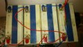
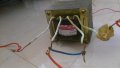
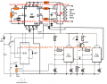
I am trying to work out an inverter design on a modified sine wave inverter which is shown in the attachment... I have tested every part of the circuit. Since i do not have an oscilloscope display with me, i am not able to cop with the waveforms, but the voltage measurements were accurately done...
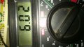
In the current design, the 555 stage at the extreme left side operates in accordance with the output clock signal from IC 4047. The Ic has been configured such that it generates stable 52 Hz flip flop frequency signals at its two output pins pin#10 and pin#11. Their tandem appearance was tested by two LEDs placed at the terminals keeping the frequency at 1 Hz. So the leftmost 555 gets 104 Hz frequency and converts it into a corresponding sawtooth waveform.. The Voltage of this waveform detected by the voltmeter is approximately 3.0 V only. Now this sawtooth waveform is being compared in IC2 with the high frequency square waves generated by IC1. The resulting signal is a PWM signal ( from pin#3 of IC2 ), which is then fed to the gate terminals of each MOSFETs using 1N4148 diodes.. SO the MOSFETs are switched in accordance with this PWM signal, resulting in a modified square wave at the output of the inverter with RMS value very much resembles to the Actual AC Voltage...
Now, My problem is ;
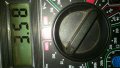
I am getting much power output ( Almost full, tested by a 100 W bulb as load ) when the PWM stage is kept disconnected . ie, the normal square wave inverter... ( 1N4148 diodes are not connected to the gate terminals ). The gate voltage shown by the voltmeter at this condion was 5.98 to 6.0 V approximately.
BUT When i am trying to connect the PWM stage (Connecting 1N4148 diodes to MOSFET gates ), the voltage at the gate terminal reduces to half ( 3.0 V ), so the output power is also getting reduced considerably.
SO What should i have to do to keep the voltage stable at the gate terminal at PWM and thereby maintaining the maximum power output ?
I have also tried using a voltage amplifier, buffer stage with Opamp etc. etc. prior to gate terminals.. But no change were detected..
I think, there might be someone to help me a lot..
I am trying to work out an inverter design on a modified sine wave inverter which is shown in the attachment... I have tested every part of the circuit. Since i do not have an oscilloscope display with me, i am not able to cop with the waveforms, but the voltage measurements were accurately done...
In the current design, the 555 stage at the extreme left side operates in accordance with the output clock signal from IC 4047. The Ic has been configured such that it generates stable 52 Hz flip flop frequency signals at its two output pins pin#10 and pin#11. Their tandem appearance was tested by two LEDs placed at the terminals keeping the frequency at 1 Hz. So the leftmost 555 gets 104 Hz frequency and converts it into a corresponding sawtooth waveform.. The Voltage of this waveform detected by the voltmeter is approximately 3.0 V only. Now this sawtooth waveform is being compared in IC2 with the high frequency square waves generated by IC1. The resulting signal is a PWM signal ( from pin#3 of IC2 ), which is then fed to the gate terminals of each MOSFETs using 1N4148 diodes.. SO the MOSFETs are switched in accordance with this PWM signal, resulting in a modified square wave at the output of the inverter with RMS value very much resembles to the Actual AC Voltage...
Now, My problem is ;
I am getting much power output ( Almost full, tested by a 100 W bulb as load ) when the PWM stage is kept disconnected . ie, the normal square wave inverter... ( 1N4148 diodes are not connected to the gate terminals ). The gate voltage shown by the voltmeter at this condion was 5.98 to 6.0 V approximately.
BUT When i am trying to connect the PWM stage (Connecting 1N4148 diodes to MOSFET gates ), the voltage at the gate terminal reduces to half ( 3.0 V ), so the output power is also getting reduced considerably.
SO What should i have to do to keep the voltage stable at the gate terminal at PWM and thereby maintaining the maximum power output ?
I have also tried using a voltage amplifier, buffer stage with Opamp etc. etc. prior to gate terminals.. But no change were detected..
I think, there might be someone to help me a lot..
Attachments
-
 275.5 KB Views: 48
 -
 101.5 KB Views: 36
 -
 97.3 KB Views: 30
Last edited: