Burned PCB of a tube amplifier (VOX AC15), help with track repair

Thread Starter

Yami

Joined Jan 18, 2016
354
Hi, I've got a VOX AC15 guitar amplifier. A conductive path between two terminals developed which caused the pcb to fry up and all the fuses were blown and also a high watt resistor was blown.

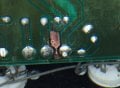
The trace which is lifted just seems to be connected to the ground plane and I don't really understand the purpose of it, maybe saving copper during the etching process? Anyway my first question is can I just removed that piece of lifted trace?

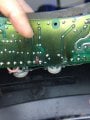
Second question is what do I do with the burned bit of pcb, its conductive. Should I cut out a hole or dig out the burned bit until its not conductive anymore. The pcb is single sided. The two terminals which are effected is TT5 and TT7.

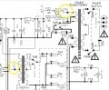
I have included a schematic of the amplifier. I have checked the components near the vicinity, I couldn't find any components which are faulty other than the 82ohm resistor (next to terminal TT5 marked as R72) which was blown. Any more tips on what to look for would be really appreciated.

The whole area was blackened and the pictures were taken after cleaning the are with IPA. I have included a pdf of the whole schematic.
Thanks in advance for the help.
 

Attachments

Last edited:

AlbertHall

Joined Jun 4, 2014
12,346
You should remove all the blackened, conductive, circuit board.

It looks like part of a ground pour so it can probably be removed but the two sections of track with red arrows are (and should be) connected by the section marked a yellow arrow so make sure this is maintained.
Picture 2.jpg
 

jpanhalt

Joined Jan 18, 2008
11,087
From the pitting on the trace, the short may have been caused by a foreign body.

In any event, I agree about removing that little section of trace. As for removing the board under it, I am less sure that is necessary. A little carbonized epoxy in a glass matrix will probably not be very conductive. I would clean well, maybe groove it, and test. Does that area get warm? A protective coating like clear acrylic lacquer would help prevent moisture from being absorbed. If necessary for resistance, a thin slot might do.

The ground pours (red arrows in post #2) are probably well connected elsewhere on the board and would not need a jumper here. Again, I would do careful inspection and testing before adding a jumper.
 

debe

Joined Sep 21, 2010
1,390
This is what i did to a PCB which suffered burns involving 240V AC. This is part of an airconditioner, I used a dremmel to grind out the carbonized PCB. I then painted the PCB with clear nail polish. When it had dried it was then covered with hot glue, due to dust & dampness. This was done a year ago & it still works.PCB.2.JPG PCB.6.JPG PCB.7.JPG PCB.10.JPG
 

Thread Starter

Yami

Joined Jan 18, 2016
354
Hi guys, just an update and need some more advice. I removed the two terminals and removed the unnecessary exposed copper track (should I remove the whole middle copper track). I chipped out the burned PCB and now there is no conductivity between the terminals. :)
I couldn't understand the point of the two thin tracks running down the bottom. But I have left it intact.
I should add I found quite a bit of dust and dead insects in side the chassis when I first opened it up. Could these be the initial culprit?
@AlbertHall what is meant by ground pour?
I need some help with figuring out what to use to fill the hole made. Would epoxy be ok? I couldn't find any good options from the local shops. All I have got is hot glue, but in my experience it doesn't give enough mechanical reinforcement. The pad on the left really needs it.
I have included some epoxy mix available at some local shops.

Before:
Before.JPG
After:

After.JPG
IMG_0701.JPG
IMG_0702.JPG

Thanks so much for all the help
 
Last edited:

AlbertHall

Joined Jun 4, 2014
12,346
That large area of copper left on the board, which will be connected to ground, is known as a ground pour. It provides a lower impedance ground connection than a track would and can also provide screening and sometimes heatsinking.

I would suggest the 5 minute epoxy (60 seconds would hardly give you time to mix it before it has gone off!).
 

Thread Starter

Yami

Joined Jan 18, 2016
354
That large area of copper left on the board, which will be connected to ground, is known as a ground pour. It provides a lower impedance ground connection than a track would and can also provide screening and sometimes heatsinking.

I would suggest the 5 minute epoxy (60 seconds would hardly give you time to mix it before it has gone off!).
Ah I see thanks, is it a good idea to generally use Epoxy for PCB repair. I did a little experiment today I wanted to check if the epoxy was conductive. I poured some into a small cap and checked it (after it was set) using a Megaohm Meter with 500V it read as >2000 Mohms but with 1000V it was significantly lower.

Thanks again.
 

AlbertHall

Joined Jun 4, 2014
12,346
The fibreglass PCB is made from glass and resin so epoxy resin should be good for board repair.
Try your test again after cleaning with IPA and drying.
 

dendad

Joined Feb 20, 2016
4,476
I have used clear fingernail polish quit successfully. There does not look to be any mechanical stress on the area caused by the track removal so just a protective cover would be ok.
 
Top