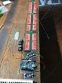
Working with shift registers (tlc5940 and Library) on Sparkfun breakout boards driving individual LEDs.
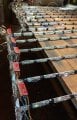
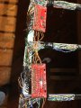
The boards are designed to connect VPRG, GSCLOCK, BLANK, XLATCH, SIN/OUT, SCLK,VCC, GND in serial. Everything works perfectly on Board #1-10. However, I need quite a few more boards/chips (up to 28) and the signals get crazy from Board 11 onwards.
I was hoping to find some (simple) options to increase the signal strengths to and past board #11, all while keeping the timing correct.. Any help with possible solutions/specific schematics is GREATLY appreciated.
The TLC breakout boards are spaced every three inches. LEDs, chips and Arduino all are powered from a 5V regulated, 40amp source (MeanWell). The connections/soldering are solid and not shorting. Each led and board has been tested individually.
I understand that this is a tall order, impedance, connections, conductance, the board, etc are in play here but I very much need to keep the boards in this lengthy configuration (necessary for art installation). Even if this boost doesn’t get all 28 chips working, I’d like to understand more how the various clock, latch, data signals can work through an extended serial bus and what I can do to clean up, bolster and push them further.
Chip Datasheet: https://www.sparkfun.com/datasheets/Components/General/tlc5940.pdf
Spark fun Board: https://www.sparkfun.com/products/10616
Attachments
-
 259.8 KB Views: 11
 -
 223.9 KB Views: 10