
Hi everyone,
Hopefully you have some thought on this weird issue I've been having.
Basically I have a mosfet acting as a switch. The end goal is to have this circuit act as a capacitive discharge welder. When on, it is essentially short circuiting a capacitor bank through a ~1 ohm resistor to limit amperage (the final design will have a much lower resistance and parallel mosfets to handle the amperage).
My problem is when the mosfet turns off, there is a HUGE negative voltage spike which kills the fet. Charging the capacitors to 24v produces an almost 300V negative spike.
I assumed this was due to inductances and tried adding diodes to kill the spike but no matter what I try nothing effects the magnitude of the spike.
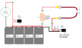
My testing layout is attached to paint a picture of what I'm doing. The Fet needs to turn on and off very quickly (will eventually run PWM at 62kHz) so options like relays or SCRs wont work.
Before anyone asks, I'm pretty much positive the routing/ layout quality of my mosfet and driver have nothing to do with this particular issue. The problem is something more substantial based on the "change one thing at a time" bounding tests I've done (below if you're curious)
Edit: I forgot to mention... at the suggestion of another forum I added an RC circuit across the drain/source. Originally I had a -300V spike and then lots of ringing, the added RC circuit eliminated that but did not effect the magnitude of the initial spike.
Hopefully you have some thought on this weird issue I've been having.
Basically I have a mosfet acting as a switch. The end goal is to have this circuit act as a capacitive discharge welder. When on, it is essentially short circuiting a capacitor bank through a ~1 ohm resistor to limit amperage (the final design will have a much lower resistance and parallel mosfets to handle the amperage).
My problem is when the mosfet turns off, there is a HUGE negative voltage spike which kills the fet. Charging the capacitors to 24v produces an almost 300V negative spike.
I assumed this was due to inductances and tried adding diodes to kill the spike but no matter what I try nothing effects the magnitude of the spike.
My testing layout is attached to paint a picture of what I'm doing. The Fet needs to turn on and off very quickly (will eventually run PWM at 62kHz) so options like relays or SCRs wont work.
Before anyone asks, I'm pretty much positive the routing/ layout quality of my mosfet and driver have nothing to do with this particular issue. The problem is something more substantial based on the "change one thing at a time" bounding tests I've done (below if you're curious)
- 3 completely different driver circuits with 3 different PCB layouts (1 good, one ok, one not so good, but all with short, fat traces). I also remade those 3 circuits on breadboards with real lazy wiring to see if there was any difference (there wasn't).
- Mosfet pcb mounted, mosfet through hole mounted on breadboard, mosfet floating at the end of ~4" wires (zero difference)
- Flyback diodes across every combination of points in the test layout (I tried multiple diodes, most recent were BYC30W-600PQ and C3D16065A-ND)
- 12 feet of 8ga wire between the two ring connectors
- 5 inches of 8ga wire between the two ring connectors
- Moving R1 to before the source pin as well as to after the drain pin
- Diode in series with drain wire
- Changing gate resistor values. Tried 2.2, 3.3, 10, 22, 100, 220, 470 and 1k ohm. Currently have a resistor/ diode to make the shut off gate resistance 220 while keeping turn on resistance 10.
Edit: I forgot to mention... at the suggestion of another forum I added an RC circuit across the drain/source. Originally I had a -300V spike and then lots of ringing, the added RC circuit eliminated that but did not effect the magnitude of the initial spike.
Attachments
-
 132.8 KB Views: 103
 -
 759.5 KB Views: 95


