Adaptive bias audio amp definition of operation

Thread Starter

Ami 2000

Joined Dec 29, 2018
6
Hello everyone.

I've recently completed the practical work on a project that had to be developed from a set of specific requirements and a restricted parts palette.

To comply with the requirements of the project, my final design includes a single ended two transistor adaptive bias audio amplifier.

The amplifier is based upon a design published by Sir Douglas Hall, K.C.M.G., M.A., in the June 1973 edition of the Radio Constructor Magazine.

A version of Halls 'Sliding Junior' circuit was constructed, but it was found that its input impedance was too low to be of use in the project, ie. the input is unable to drive the adaptive bias circuit, and the output clips.

To circumvent the problem a follower could be added at the input, but to maintain the project transistor count to the limit in the specific, a feedback capacitor was added instead, so that the amplifier output would bootstrap the adaptive bias circuit effectively raising the input impedance.

So far so good.

The problem I have is that the working hardware has been presented along with the paper with the description of operation. The paper was returned, twice actually, with a note on this occasion that the tutor felt that the description of the amplifier was incorrect, particularly the claim that it was "bootstrapping" the adaptive bias diode clamp circuit, and that if I couldn't correctly describe the function of the circuit, he could only conclude that the hardware was not in any part my work.

The above is in essence my problem and the question is am I wrong? If so, how should I describe the method of operation. If on the other hand the tutor is wrong (and he refused to say how he thinks the circuit works), it will be catch 22 on getting no marks if I try proving it!

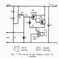
I've attached the circuit diagram of the amplifier as built.
slider amp v2.01-1.JPG
Any opinions welcomed.

Thanks for reading,
Ami.
 

Thread Starter

Ami 2000

Joined Dec 29, 2018
6
Hi.

Yes, that's the one.

I semi plagiarised the authors (not very accurate) description in my first attempt at the paper, and was canned for that as well.

I'm sorry not to give too much away here, just the salient points, as I've posted detail elsewhere, and it just descended quickly into off topic discussion.

Thanks,
Ami.
 

ericgibbs

Joined Jan 29, 2010
18,845
hi Ami,
Please post the written submission that you made which was considered incorrect so that we can check your work.
E
 

Thread Starter

Ami 2000

Joined Dec 29, 2018
6
Hi

hi Ami,
Please post the written submission that you made which was considered incorrect so that we can check your work.
E

Not at home at the mo. But will post the relevant section as soon as I can, though the essentials are in the first post.

Thanks,
Ami.
 

bertus

Joined Apr 5, 2008
22,276
Hello,

The original schematic is using an output transformer:

Sliding junior amplifier.png

The way you have posted does not adapt the impedance.

Bertus
 

Thread Starter

Ami 2000

Joined Dec 29, 2018
6
Hi.

Hello,

The way you have posted does not adapt the impedance.

Bertus
Love the cat!

Having gone to great lengths to acquire a transformer to try in the "Hall" circuit, it was found that its value was only that it prevented DC in the speaker voice coil and also increased the efficiency. The spec of that transformer gives almost unity transformation impedance load at the transistor collector, (it was actually a gapped core transistor driver transformer designed for push pull output stages).

I was able to obtain a gapped core audio inductor for my version and just used a capacitor to couple the speaker, had we been allowed to use a higher supply voltage and more active devices in the design I wouldn't have even considered an inductor loaded SE amplifier, its basically just there to improve efficiency.

The circuit works well, that's not my problem.

Thanks,
Ami.
 

Thread Starter

Ami 2000

Joined Dec 29, 2018
6
Hi

hi Ami,
Please post the written submission that you made which was considered incorrect so that we can check your work.
E


Here's the assignment.
.................

The term practical work project is to research and build a design for a functional radio receiver, the requirement for the completed set is that it can resolve local stations transmitting on the medium wave band with good selectivity and clarity, the test of sensitivity will be its ability to receive a 1KW station 100Km distant without any external antenna The design can be original or preexistent but the student must have built it and be able to demonstrate understanding of its function.

The technical specifications of the receiver are that it:

1. Should be transportable and self contained.

2. Be powered by primary cells, at a nominal maximum of 3volts.

3. Will include no more than 3 active devices. They will be bipolar transistors, and can be selected from types BC327, BC337, BC549, BC559, in any combination.

4. Will drive a loudspeaker so it can be used by multiple listeners.

5. Incorporate in its design an automatic method by which its battery power consumption is demonstrably economised, at low sound volume.

Marking will be by grade average and will be judged by:

6. Sensitivity.

7. Selectivity, its ability to separate signals.

8. Sound quality.

9. Maximum achievable sound level meter results before the onset of output clipping.

10. Economy, cost of battery cell's divided by hours running time, at a specific "volume" (Extrapolated from consumption and manufacturer data on cells capacity).
….…………..............

The following is an extract from the overview that I wrote on the design. I've only included the audio amplifier part, the tutor dismissed the explanation of the adaptive bias operation as nonsense.

Here it is....

**********************

....with regards to the audio stage, it would be necessary to realize it with just two transistors.

To that end the "Sliding junior" amplifier (Radio Constructor magazine, June 1973), designed by Sir Douglas Hall was investigated, (see first attachment).

attachment 1sliding junior.jpg

This design is based upon the idea that the input signal is AC coupled to a diode clamp circuit that has the effect of superimposing the signal on the amplifier bias so as to increase drive for the transistors in sympathy with the instantaneous input level. The author claimed that this "feed forward sliding bias" arrangement ensured that there was always sufficient bias to keep the amplifier in a linear (class A) part of its transfer curve, without the high dissipation normally associated with fixed class A topologies, whilst also providing better sound quality than a class B amplifier at low volume settings.

Although the design did work when built near faithful to the original as was possible, the claims of the author proved to be inaccurate, as the design suffered from an unusual distortion that is a product of the gain being dependant on the current through the output transistor, controlled by the instantaneous input level.

Another drawback noted was that on occasions the design was unable to stay fully in class A operation. This was found to be due to a transient lack of bias, sounding to the listener much like cross over distortion in the class B amplifier over which the author claimed his design had superiority. The reasons for this turned out to be quite complex and lay with the nature of the input signals. The amplifier performance was adequate on signals that comprised complex high energy content such as orchestral music, but was unsatisfactory with low energy, or discontinuous content, for instance speech or solo guitar. This was also more noticeable with increased impedance of the signal source output, and it would have been necessary to include a follower stage at the input, increasing the transistor count.

The last flaw in the design that was addressed was the inclusion of an output transformer, this component was assumed to be included to provide coupling to the speaker without the latter needing to pass the standing DC current of the output transistor. As a feature, this component was historically also associated with an impedance matching role, though in a design of this supply voltage, it isn't necessary, it also introduces losses and distortion. DC blocking by a large value capacitor being a suitable alternative. The load for the output transistor remained inductive in the final version however as it suited the requirements of maximum achievable efficiency and output power with the limited supply voltage and restrictions on active component count.

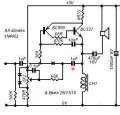
The solution to the drawbacks noted was the adoption of another method of providing adaptive bias in sliding bias amplifiers that Sir Douglas Hall dismissed as inferior. In early incarnations of this topology, a proportion of the amplifier output is fed back via a diode/capacitor combination providing a DC level that is then used to bias the output stage of the amplifier. An example of this early topology is seen in the second attachment, and is a design attributed to Phillips.

Attachment 2slide1.gif

A major difficulty with this method is that the smoothing capacitor's value is a compromise between being sufficiently large so as to prevent unwanted feedback of the audio signal, and small enough that the circuit's transient response prevents noticeable distortion due to insufficient bias. The suboptimal performance that was a result of this tradeoff contributed to the topology's unpopularity as they couldn't be expected to deliver more than "public address" standards of fidelity.

The final version of this design instead feeds back the audio as an AC signal through a capacitor, and adds its negative transitions to that set by the idle current potentiometer that controls the initial DC level of the diode clamp that operates as a envelope follower, tracking the input signal. This bootstrapping action effectively increases the input impedance and provides bias drive that up to the circuit limitations, keeps the amplifier working in its most linear region. In listening tests, there was also no discernable lag in transient response. The only adjustment of this dynamic bias needed is the choosing of a suitable value capacitor, however unlike the previous method mentioned, it seems in no way critical. In this example, a value of 0.47uF provided barely sufficient bias, whereas increasing to 10uF began to cause unnecessarily high dissipation. The final circuit uses a component of 1uF.

With regards to the bias/gain dependant distortion, an audio quality and thermal stability improvement was gained from including an un-bypassed 0.33ohm degeneration resistance. This resistor provides a degree of DC negative feedback, (approximately 10% of output) that improves gain linearity as it progressively removes bias from the BC 559 base with increased output stage current, this also aids the thermal stability.

The topology in the final version to my knowledge has been tried by at least two others, (note 1 & 2), who confirmed that its transient response is superior to any other sliding bias amplifier that has anywhere close as low a component count.

The final version of this circuit is shown in the third attachment.

attachment 3slider amp v2.01-1.JPG

It should be noted that this amplifier is deliberately sub optimal regarding output power, mainly because of the output transistor that had to be used (600mW max total dissipation), it also follows that the distortion figures are taken well away from the onset of output clipping. The frequency response is also deliberately limited because of its intended use, (AM radio), it was found that restricting this made for a more pleasant experience as it attenuated the level of the annoying heterodyne whistles that plague AM radio.

Although this amplifier topology will in all honesty never be worthy of the title HiFi, it does sound quite respectable. After the current project, I would like to investigate the possibility of a higher powered version, just to see if it could be done.

Norman Preston (note1) also supplied the following figures that are results from his testing the amplifier.

At 1KHz sine.

Output power = 120mW ave into 3R at an input of 100mV and supply of 3volts.

THD+noise = 3% at 120mW

Frequency response = 120Hz - 8KHz +/- 3db

Efficiency = approximately 30% (supply current of 130mA at 3volts full output)

Note 1. Thanks to Mr Norman Preston, who worked for HMV, S.Smith Accessories, (Radiomobile Ltd, London) during the nineteen fifties and sixties as a car radio designer.

Note 2. Thanks to Mr Don Field, RF technician and technology journalist.
 

Thread Starter

Ami 2000

Joined Dec 29, 2018
6
Hi.

Well this was another waste of time.

I conclude that I'm either very wrong, and this is polite silence, or, right and no one wants to cross an anonymous educator?

I've just spent three days of my winter holidays writing up an patent style in depth description of operation to append to the overview, (even though we weren't asked for one), to try to reinforce my adhering to its contents, which is what I now intend to do. I'm quite mercenary enough to write another filled with whatever garbage the tutor would want to see, if I achieved a grade, if only he would let me know what that particular garbage is.

Administrator.
Please close this thread and delete my account.

Thanks, Ami.
 
Top