
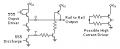
For years I've been trying to figure out a way to do this for years on a standard (not CMOS) and I think I've got it, The 1.2V V+ drop on the bipolar 555 positive rail.

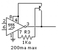
Since the - rail is usually reached on a stock 555 all I really needed was the positive rail pull up, which this should nicely. It allows for much greater drives like so:

Definitely less elegant than I was hoping for, but I'll test it out <Sigh> Yet another revision.
Since the - rail is usually reached on a stock 555 all I really needed was the positive rail pull up, which this should nicely. It allows for much greater drives like so:
Definitely less elegant than I was hoping for, but I'll test it out <Sigh> Yet another revision.
Attachments
-
 1.4 KB Views: 52
 -
 2.8 KB Views: 49
 -
 1.6 KB Views: 30
 -
 2.9 KB Views: 31
Last edited:


