
Hi all,
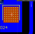
I keep getting the error Clearance constraint (collision < 0.254mm) between via on multilayer and pad on top layer". The top layer is a thermal pad, bottom layer is a copper plane that is connected to the cathode of the diode. It is a Cree SiC diode, and it should not be connected to ground like most other thermal pads. I am using 0.3mm holes to connect the two layers and keeping the bottom layer copper plane as big as possible before it violates clearance constraints. But this error I've only recently started getting when I reduced the clearance rules to start routing some lower voltage sections of the board (the voltage on the diodes are about 1.2kV each).
Can anyone help to explain why I am getting these errors even though I reduced the clearance constraints? They were working fine when the clearance rules were set to 3.2mm. I understand that this is some kind of bug for Altium but I still have not found a way around the bug to get rid of these errors scattered around my board. The nets for the vias are all set to the same net as the bottom layer copper pour and the top layer thermal pad of the diode. So I do not see why it is throwing errors. I also have the rules set to ignore clearance between same net components.
Regards, SiC
Attachments
-
 221.8 KB Views: 3


